Lattice Radiant iCE40 UltraPlus Project Setup
Project Setup
Open Lattice Radiant. If you are prompted for a license file, navigate to it. See the Radiant install instructions if needed.
Create a new project and name it “iCE40_demo”. Select the project location in the directory you wish. Make sure that the path does not include spaces since this often leads to errors later in the synthesis process. You do not need to add any existing HDL files to the project.
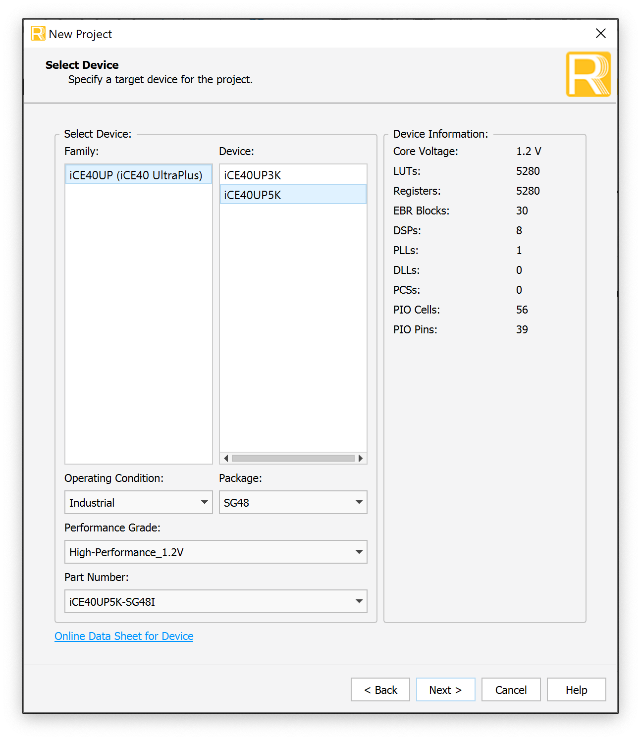
In the “Select Device” menu, select the iCE40UP5K and the SG48 package. On the next page, select Lattice LSE as the synthesis tool.
Project Implementation
After the new project wizard completes, you will be presented with the following default screen.
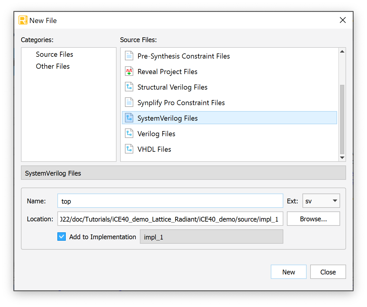
Navigate to File > New > New File and select SystemVerilog Files in the New File selection window. Name your file top and click New to create the file.
Implementing the Design in SystemVerilog
In this demo we will write HDL to blink the onboard LED at ~1 Hz.
To do this, we will use the on-board iCE40 high-frequency oscillator to generate the clock signal and build a simple counter which will toggle at the desired frequency.
Save the file and click the green play button in the GUI to run the synthesis process.
module top(
     input   logic reset,
     output  logic led
);

   logic int_osc;
   logic [24:0] counter;

   // Internal high-speed oscillator
   HSOSC #(.CLKHF_DIV(2'b01))
         hf_osc (.CLKHFPU(1'b1), .CLKHFEN(1'b1), .CLKHF(int_osc));

   // Counter
   always_ff @(posedge int_osc) begin
     if(reset == 0)  counter <= 0;
     else            counter <= counter + 1;
   end

   // Assign LED output
   assign led = counter[24];

endmodule
Note that we configure our reset to be active low (reset when 0 or connected to ground) since we have internal pullup resistors which make it easy to pull the pin high but not internal pulldown resistors.
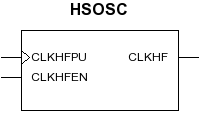
In this design we use the HSOSC module which is the high-speed oscillator available on the iCE40UP5K chip. The HSOSC module is a Verilog library that is provided with the iCE40 device support package in Radiant. You can find more information about the oscillator under Help > Lattice Radiant Software Help > Reference Guides > FPGA Libraries Reference Guide > Primitive Library - iCE40UP (iCE40 UltraPlus). Here, as an example of how to infer a modules with parameters in Verilog, we instantiate it with the optional parameter CLKHF_DIV which sets the output frequency to 24 MHz.
Netlist Analyzer
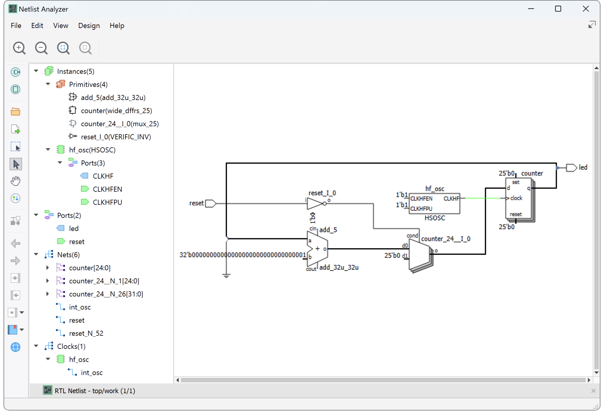
After synthesizing your design, it is worth taking a look at the Netlist Analyzer. This tool provides a block diagram view of the design. This is a helpful tool to make sure that the Verilog you wrote is implying the hardware that you intend. Remember that as a digital designer you should always think about the underlying hardware and simply write the Verilog idioms to imply it. Approach HDL like a traditional programming language at your peril!
If we look at the Netlist Analyzer (found under “Tools > Netlist Analyzer” or the green and black icon in the toolbar), we will open a window which shows a block diagram. We see that we have implied an adder, a mux to control the value to the registers, the HSOSC module, and a 25-bit-wide register.
Resource Usage
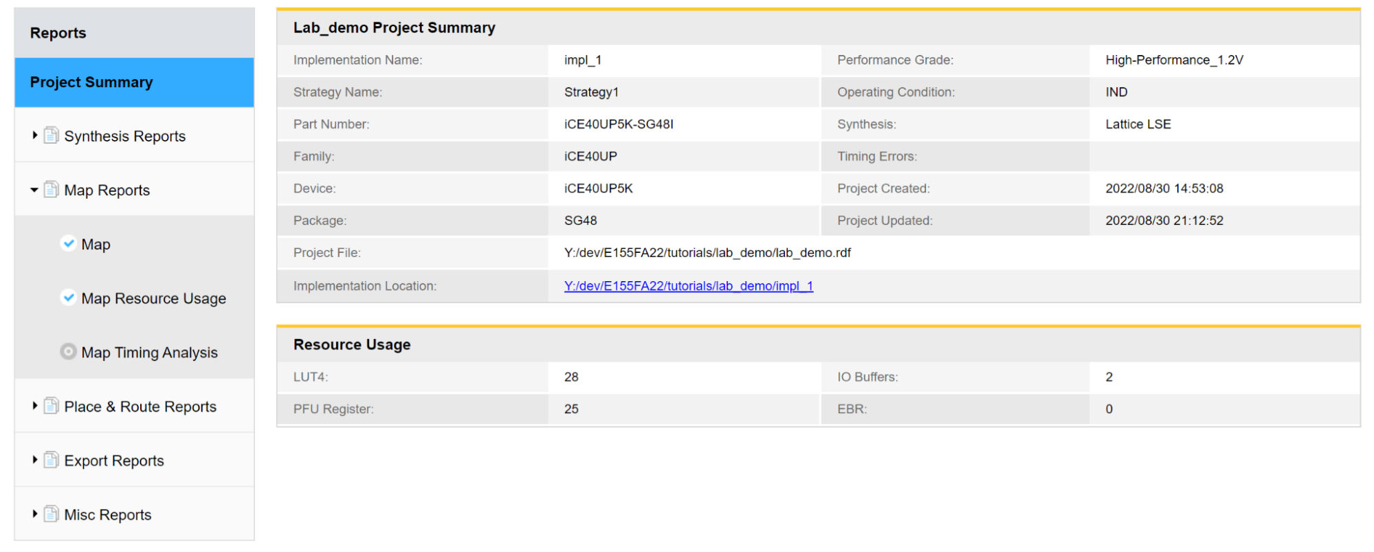
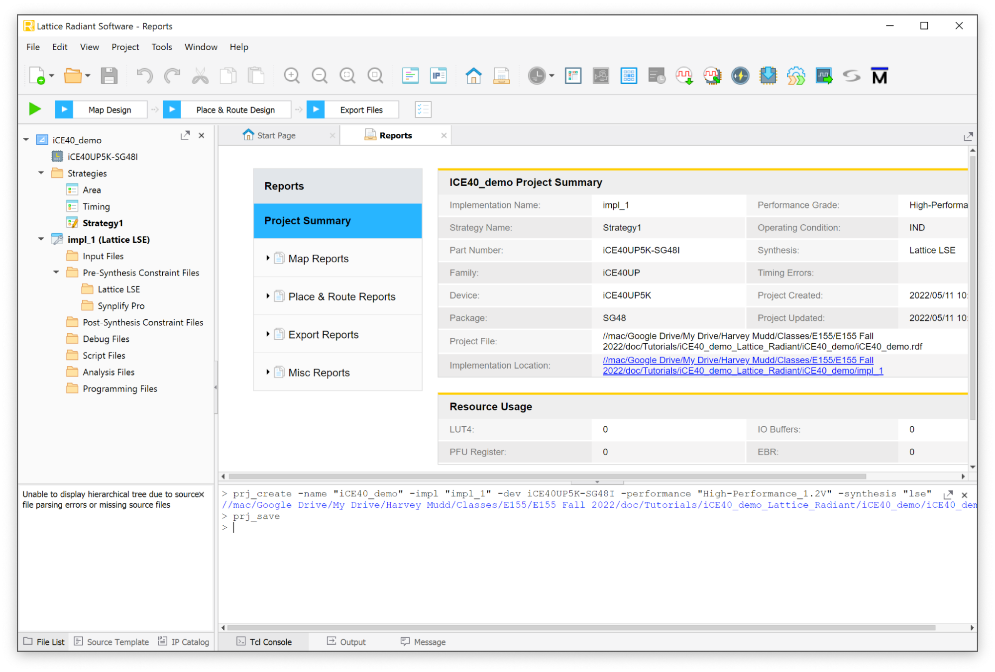
There is also some useful information in the Reports tab under Project Summary in the Resource Usage section. In particular, this section will show us the number of registers, look-up tables, IO buffers, and embedded RAM blocks (EBRs) that we have implied in our design. For this design, we have 25 registers for storing the current count. An additional 3 logic cells are needed for their LUT4s to provide the additional logic (adder, mux, inverter).
Device Assignment: Device Constraint Editor
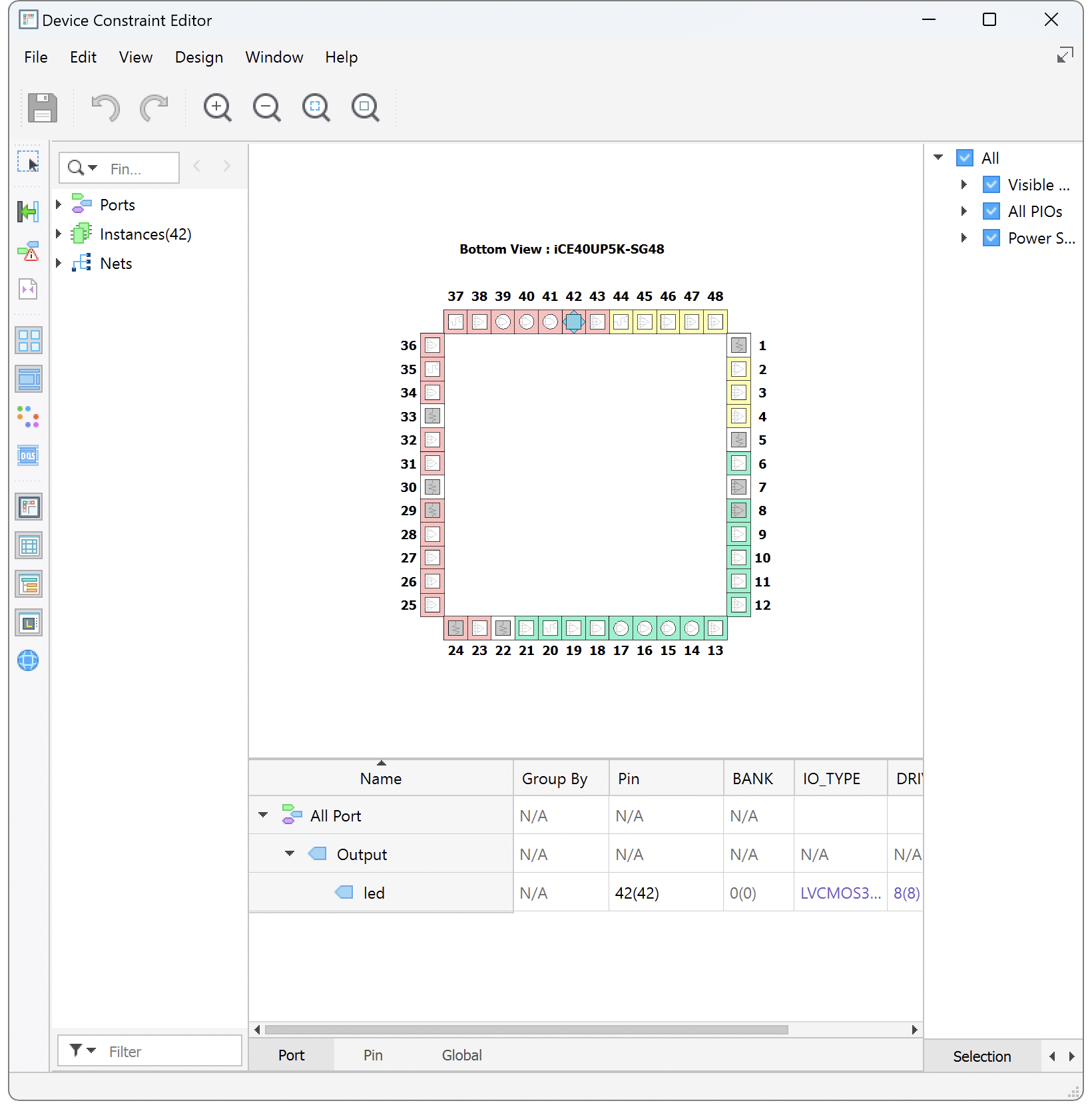
When you first synthesize the design, the inputs and outputs of your top-level module will be randomly assigned to I/O pins. Next, you need to set the pin assignments to route the signals to the I/O pins that you desire.
Open the Device Constraint Editor and find the signal name and assign it to your desired pin. In this example, we will route the “led” output to GPIO 42. Select the table entry in the “Pin” column associated with the LED signal and enter “42”. You will notice that the currently routed pin is labeled in parentheses, 36 in this example. To update the design to route to our desired GPIO pin, we need to resynthesize the design. Click the green play button again to run the toolchain. When you do this for the first time, you will be asked to save a .pdc (pin device constraint) file. Name and save the file. After synthesis completes, open the Device Constraint Editor and confirm that the desired and routed pins match. In this case you should see “42(42)” in the table entry corresponding to the led output.
Device Programming
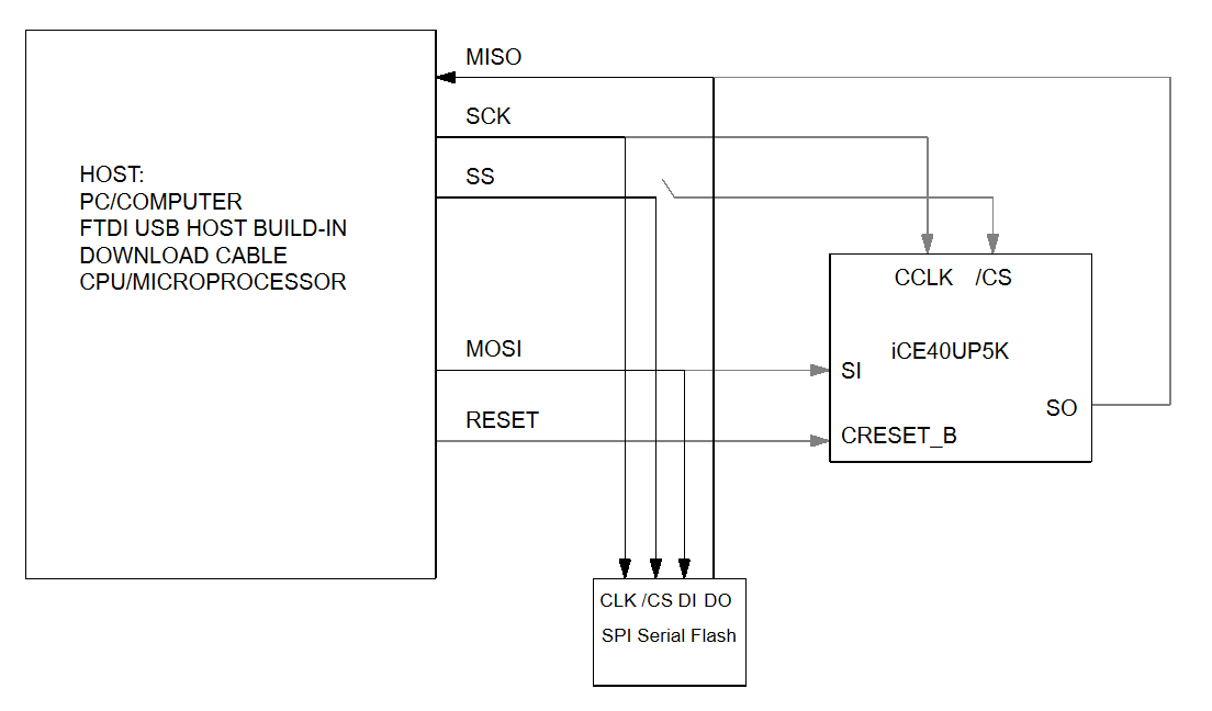
To get our design working on our board, we need to program it to the flash memory onboard the UPduino board.
Each time the FPGA powers up or resets, it reconfigures itself over a serial peripheral interface (SPI) connection from a binary (.bin) configuration file on a flash memory chip.
To program the device, we need to set up the programmer to put the .bin file that is generated by our synthesis tool onto the flash chip.
Click the button in the toolbar to open the programmer (the icon is the chip with a blue arrow pointing downward) or using the menu Tools > Programmer.
Connect your UPduino board to your computer and click the “Detect Cable” button in the “Cable Setup” sub-window on the right of the Programmer window. You should see a message noting that “INFO - Board with FTDI USB Host Chip detected.” in the output window. If the host chip is not detected, you may need to install FTDI drivers for the device.
Next we need to correctly configure the programming toolchain to program our device. By default, the UPduino board only enables programming of the flash chip on board and not the onboard compressed random access memory (CRAM) of the FPGA itself. To do this, highlight the device in the list view and open the “Device Properties” window either by using the icon in the toolbar (chip with pencil on top) or by right-clicking on the entry in the table and selecting the “Device Properties” option.
Change the default entries to the following selections:
- Set Target Memory to
External SPI Flash Memory - Set operation to
Erase, Program, Verify - Under SPI Flash Options set
- Family:
SPI Serial Flash - Vendor:
WinBond - Device:
W25Q32JV - Package:
208mil 8-pin SOIC
- Family:
After configuration, the block diagram should look like this.
After updating the configuration, you are ready to program the device. (Note: on your first run, you may get a firewall warning that a new program “cableserver” is being run and needs access. Allow access to the program.)
You should see a series of outputs printing in the output window as the programmer cycles through the various pieces of the programming process (initialization, enabling, erasing, programming, verifying, etc.). After the programming finishes, you should see a message that the programming operation was successful.
Testing in Hardware
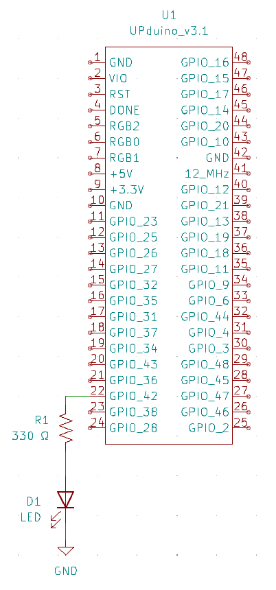
If you are using the E155 development board, you should see the onboard LED connected to P42 blinking. If you would like to test the hardware separately with just the UPduino you can unplug the USB from your board and connect your UPduino board to a breadboard, wiring up an LED in series with a current limiting resistor (typically a value between 330 Ω and 1kΩ is a good choice). Then, reconnect your board to power via USB or using the +5V input on the board from a DC power supply.