Lab 1 Specifications
Introduction
In this lab you will familiarize yourself with the microcontroller unit (MCU) and field-programmable gate array (FPGA) development boards we will be using this semester.
Learning Objectives
By the end of this lab you will have…
- Assembled your development board for the class and tested out your MCU and FPGA boards.
- Written a Verilog module to control LEDs and a 7-segment display.
- Programmed the FPGA with Verilog code.
- Gained confidence in building, assembling, testing, and debugging circuits.
- Interfaced a 7-segment display to the board.
Requirements
Follow the steps in this guide to test your FPGA and MCU boards. Write some Verilog code to exercise the FPGA using the switches, LEDs, and a 7-segment display to ensure your board is operational. Simulate and synthesize your code, then upload it to the flash memory and re-test the board. Hook up a 7-segment display and demonstrate that it works.
Resources
Specs
Lab-specific Specifications
Proficiency
Excellence
General Specifications
Proficiency
General Schematic Specifications
Block Diagram
HDL & Code Specifications
General Formatting
Comments
Lab Writeup/Summary
Excellence
General Schematic Specifications
HDL & Code Specifications
General Formatting
Testbenches
Lab Writeup/Summary
Before You Start
Before you start working on this lab, you should familiarize yourself with the documentation for both the UPduino v3.1 and Nucleo-L432KC boards. The website has links for the UPduino v3.1 User Guide and the Nucleo-L432KC User Manuals on the Resources tab. These two documents contain information that will be helpful for answering questions that you may have during the course of this lab.
Background
In the 1980’s and 1990’s, digital design projects were built from a truckload of chips, each containing a few logic gates such as 74xx series logic gates or simple programmable array logic chips (PALs). Such projects involve placing and wiring together dozens of chips on a breadboard. It was easy to make a wiring mistake or burn out a chip and spend hours tracking down the problem. Now you can perform all of your digital logic on a single field-programmable gate array (FPGA) to greatly reduce the necessary wiring and number of chips. Later in the course, you will use the Cortex-M4 microcontroller to write programs in assembly language and C that can interface with external hardware and the FPGA.
Nucleo-L432KC Development Board
The Nucleo-L432KC development board provides a convenient platform to test and develop embedded systems applications. The board is focused around an STM32L432KC MCU and provides voltage regulators to provide power to the chip, various breakout headers which allow access to the pins of the microcontroller chip, a reset button and user input button, configuration jumpers, and an embedded ST-LINK programmer/debugger.
Programming
The STM32L432KC has an embedded ST-LINK/V2-1 programmer and debugger as described in the Nucleo-32 User Manual. The main purpose of the ST-LINK is to provide the ability to interface with the serial wire debug (SWD) interface of the MCU via USB.
There are a variety of integrated development environments (IDEs) which can be used to interact with the device including PlatformIO, Keil μVision, and SEGGER Embedded Studio. The IDEs provide a helpful wrapper around compiler toolchains such as GNU Compiler Collection (GCC) toolchain to facilitate easy programming and debugging. In this course you are welcome to use any IDE you would like, although instruction and support will be focused around SEGGER Embedded Studio which is based on the GCC toolchain.1
UPduino v3.1 FPGA Development Board
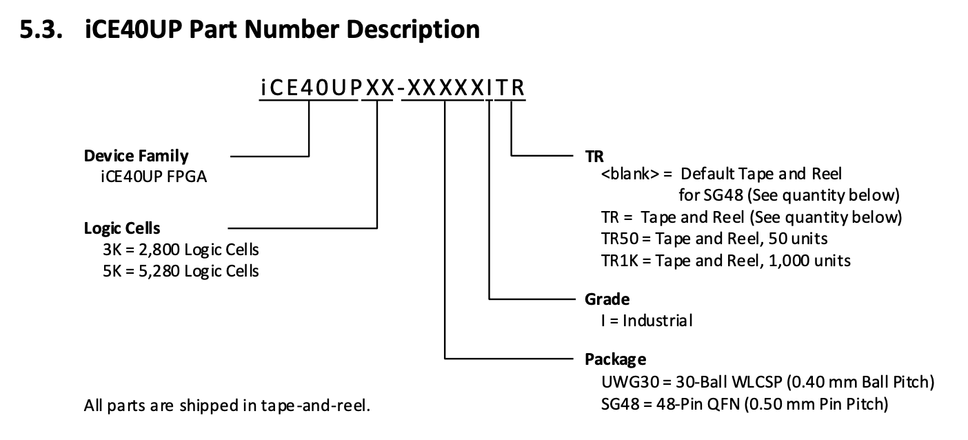
The UPduino v3.1 is developed by tinyvision.ai and designed around a Lattice Semiconductor UP5K field programmable gate array (FPGA). Section 5.3 of the iCE40 UltraPlus Family Data Sheet (FPGA-DS-02008-2.0) explains the naming of the chip.
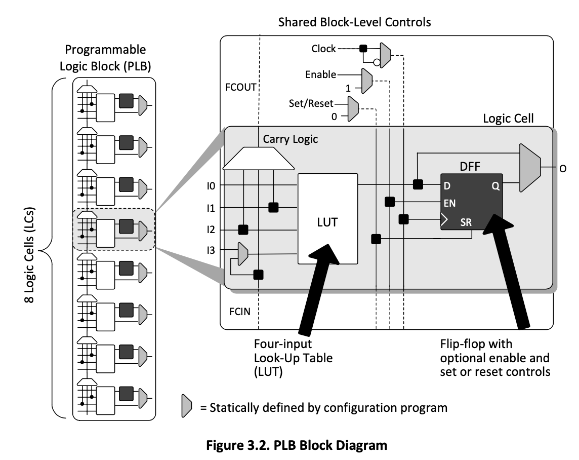
The Lattice UP5K is very similar to the Cyclone IV architecture that is used to introduce FPGAs in E85. At its root, the FPGA consists of Logic Cells (Lattice’s version of the Intel/Altera Logic Elements you learned about in E85) which can be internally connected within Programmable Logic Blocks (PLBs) within the FPGA to form digital circuits. Each Logic Cell (LC) consists of a 4-input look-up table (LUT) and a programmable D flip-flop, along with additional clock control and carry logic. Figure 3.2 from the FPGA datasheet shows the basic architecture of a PLB and LC.
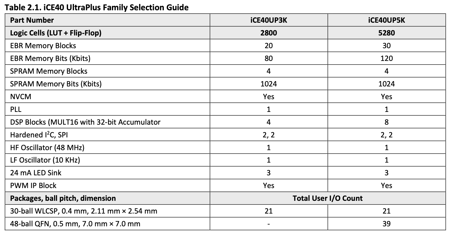
The UP5K on our UPduino v3.1 board is the 48-pin QFN package. As you can see from the table, it contains 5280 logic cells, 30 Embedded Block Ram (EBR) Memory Blocks of 4 Kbits each, 4 256-bit Single Port synchronous RAM Memory Blocks, and an on-board high-frequency (48 MHz) and low-frequency (10 kHz) oscillator.
Digital Design Synthesis and Programming
The FPGA is programmed using the onboard programmer via the synthesis tool Lattice Radiant. After setting up and compiling the Radiant project, Radiant will generate bitstream files which are used to configure the FPGA.
More details will be provided later in this lab writeup.
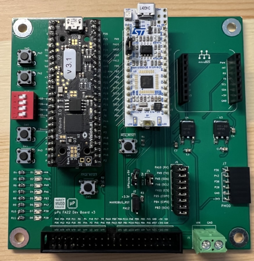
E155 FA22 Development Board
In this lab you will assemble a custom printed circuit board which hosts the MCU and FPGA boards. The board has several features that will be convenient for developing embedded systems such as:
- Pins which can be directly routed from the MCU to the FPGA via the board
- Extension headers for the mikroBUS and 6-pin PMOD standard
- User configurable LEDs, pushbuttons, and slider switches.
- Header to route pins via a ribbon cable to a separate breadboard adapter PCB which can be inserted into a solderless breadboard.
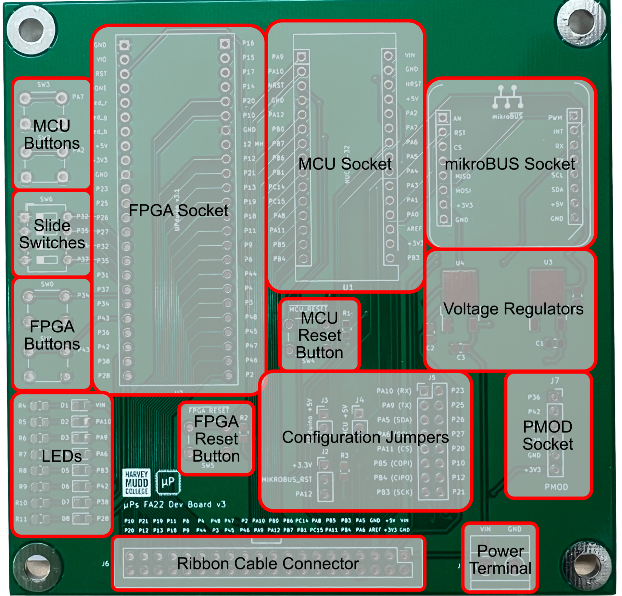
The board has several main sections that you should make yourself aware of. They are annotated in the image above.
- Voltage Regulators and Power Terminal: A +5 V (NCP1117DT50RKG) and +3.3 V (NCP1117DT33T5G) low-dropout (LDO) voltage regulator which is used to regulate the input provided via the power terminal on VIN. Make sure to check with the schematic to ensure that you put the regulators in their proper places. See Powering the Board for more details.
- FPGA, MCU, mikroBUS, and PMOD sockets: These sockets are populated with female headers for the MCU, FPGA, and other extension sockets to be plugged into.
- Reset Push Buttons: The reset pushbuttons are connected to the reset inputs on the MCU and FPGA respectively. The MCU reset button will cause the code to begin execution from the first instruction. The FPGA reset button causes the FPGA to reconfigure itself from the on-board RAM which stores the configuration file for the design you have uploaded.
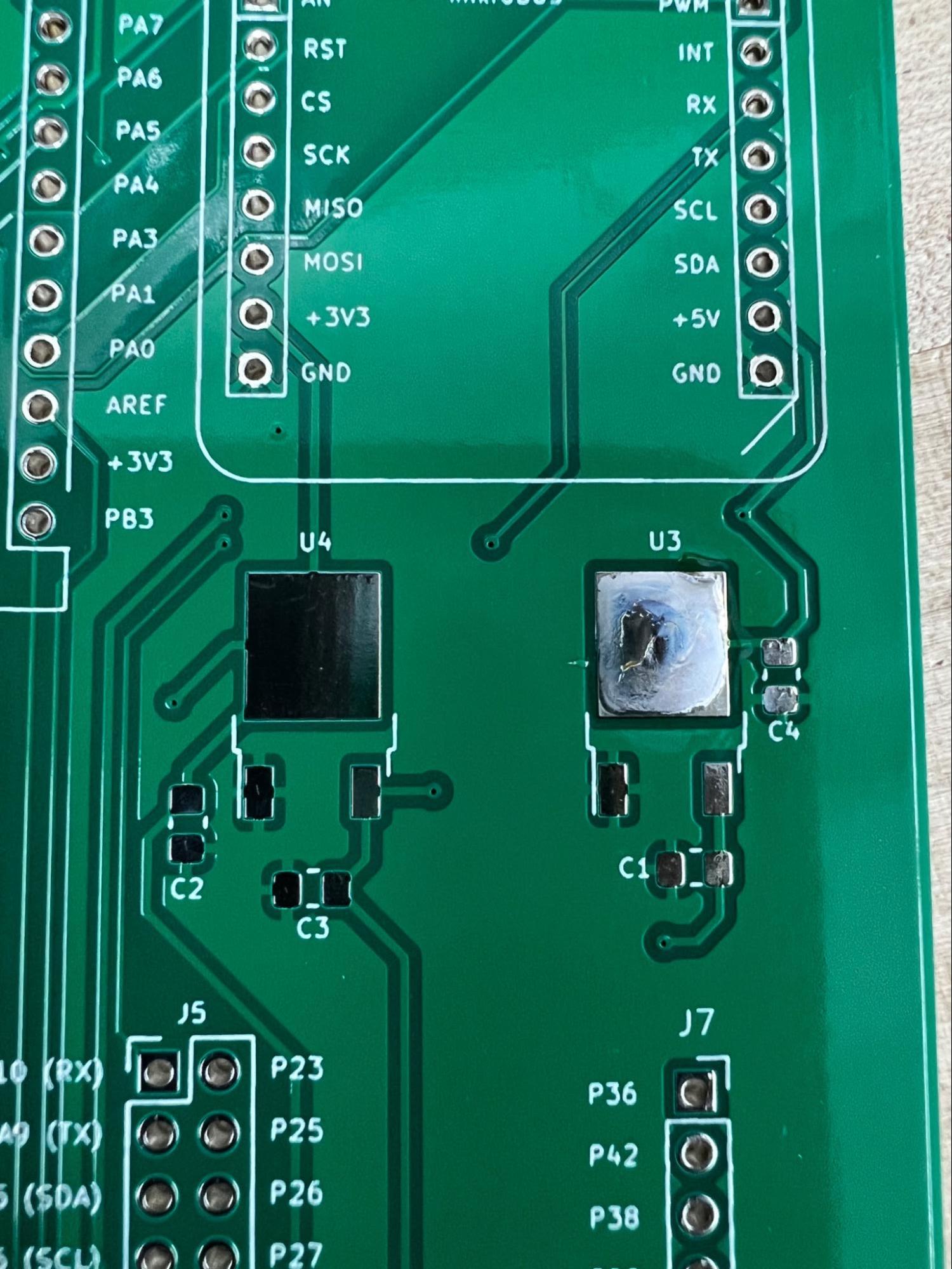
- Configuration Jumpers: The configuration jumpers on the board allow you several options to set the power and signal connections for the MCU and FPGA. J2, J3, and J4 control the mikroBUS reset signal and the power for the FPGA and MCU boards respectively. The mikroBUS reset signal can also be connected to MCU pin PA12 to enable the MCU to reset the connected peripheral via software. The configuration jumper J5 is a 2x8 header with MCU pins on the left hand side and FPGA pins on the right hand side. Note that on the 2023 version of the board, J5 has been replaced with an 8-pin DIP switch with the reference designator SW7. The functionality however, remains the same as the jumper. By attaching a jumper between the pins in the same row, the MCU pin on the left side of the jumper can be directly routed to the FPGA pin on the right hand side via traces on the PCB. This allows for convenient and high-fidelity interfaces between the MCU and the FPGA without the need for external wires.
- Ribbon Cable Connector: The ribbon cable connector is used to route a subset of the MCU and FPGA pins out to a cable which connects to the breadboard adapter board.
- MCU, FPGA, and Slide Buttons: The push and slide buttons on the board are routed to pins on the MCU and FPGA in order to provide on-board options to toggle GPIO pins on the respective devices. Note that all of these buttons are configured as active low (i.e., closing the switch connects the pin of the device to ground) without any hardware pullup resistors. In order to use them, you must configure the internal pullup resistors on the MCU or FPGA in order to avoid floating logic levels.
Assembling the Board
In this section you will walk through the steps to assemble your board. The PCB has both through hole technology (THT) and surface mount technology (SMT) parts. SMT parts are generally preferred on PCBs since they are more compact and easier for machines to solder although THT parts are typically easier for beginners to solder. If you haven’t done much (or any!) SMT soldering before, don’t worry! One of the points of this lab is to give you a chance to develop this skill!
All the parts you need to build your board are provided in your kit bag. Typically, it is easiest to start with the SMT parts before soldering the THT parts since the board will lay flat. So we’ll start by soldering the SMT components.
Assembly Tips
Soldering is a skill that you need to practice just like anything else. The most important thing to remember when soldering is that it is roughly 100x easier to solder than to desolder a component. So, whenever possible, make sure that you align the component correctly before soldering all the pins. Often the best way to do this is to solder a single pin on one side and then confirm that the component is correctly aligned before soldering the rest of the pins. If something is misaligned, then this will make it easy to correct since you only will need to reflow a single solder joint. A few additional tips:
- Soldering often will make you wish you had another hand or two. Soldering SMT components in particular can be a bit tricky because you need to hold the component with tweezers to align it. A good strategy is to first melt a little bit of solder on one of the pads and then grab the component with tweezers while holding the iron in your other hand to reflow the solder and align it.
- When soldering THT headers like those used for the sockets, make sure that the headers are oriented correctly (most of the time perpendicular to the PCB surface). One tip is to insert a strip of male headers into a breadboard and then attach the female headers and set the PCB upside down on top of the male headers to solder them. If you do end up making a mistake and need to desolder a strip of header pins, the plastic shroud can be removed in order to let you pull out individual pins. See this YouTube video for an example. Although in the video he shows the example for a male header pin strip, you can do the same thing with a female strip as well.
Suggested Soldering Order
Below is a recommended soldering order.
- Solder the voltage regulators. Put a bit of solder on the big square pad and reflow while bringing the regulator on top in order to solder it. You can apply heat to the pad via the metal edge at the top of the regulator.
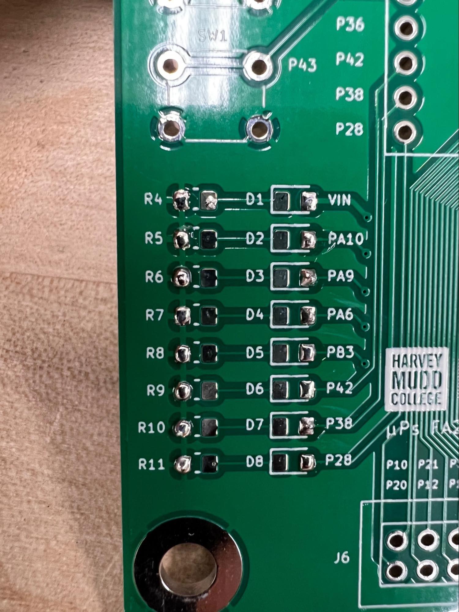
- Prepare to solder the remaining SMT components (resistors, capacitors, and LEDs) by applying a small amount of solder to one pad of the SMT footprints R1-R11, C1-C4, and D1-D8..
- Solder the decoupling (also known as bypass) capacitors C1-C4 around the regulators. These are used to smooth out any transients and ensure smooth, constant voltages. These capacitors have no polarity, so either way is fine.
- Next, solder the resistors on the board. Pay careful attention to make sure that you solder the correct resistors by referring to the board schematic (available on the course website).
- Next solder the LEDs. The LEDs are polarized, so you’ll need to make sure to solder them the right direction or they won’t work. There is an arrow on the bottom of the package which indicates the direction of the current flow from the anode to the cathode. Again, refer to the schematic for proper alignment. When looking at the PCB with the text facing upright, the cathode should go on the left hand side (connected to its current limiting resistor). There are three different color LEDs. D1 is red (VIN), D2-D5 are green (connected to the MCU), and D6-D8 are blue (connected to the FPGA). After finishing this step, you are finished with all the SMT components!
- Now it’s time to tackle the THT components. Put the components into their respective places and solder them in. Pay careful attention to ensure that the female header strips are correctly aligned and perpendicular to the board. You will need to snap off 2- and 3-pin headers from the provided 40-pin header strip in order to populate J2-J4. The easiest way to do this is to use a pair of needle nose pliers to snap off the right number of pins.
- After finishing the main development board, follow the same procedure to assemble the breadboard adapter PCB.
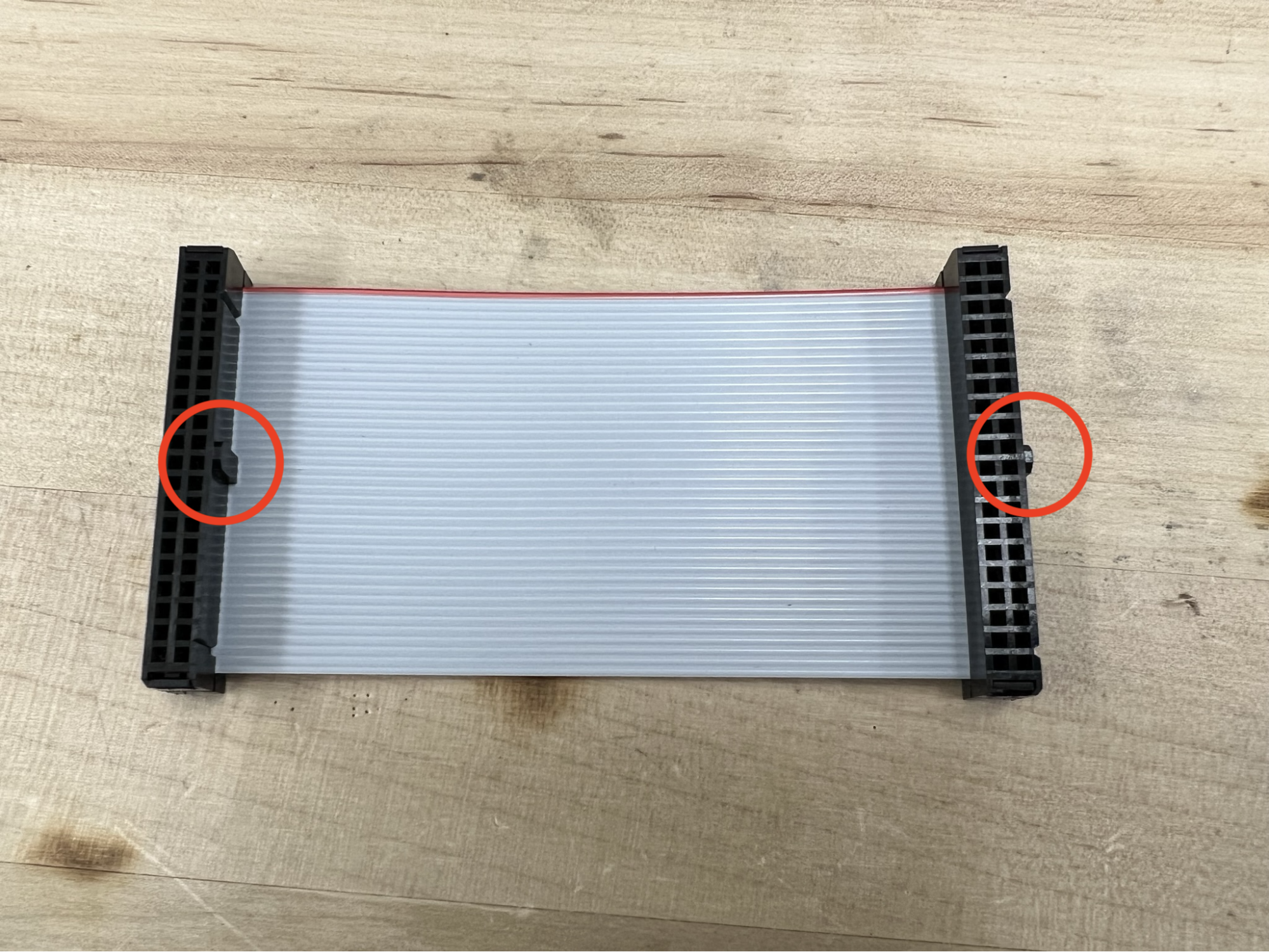
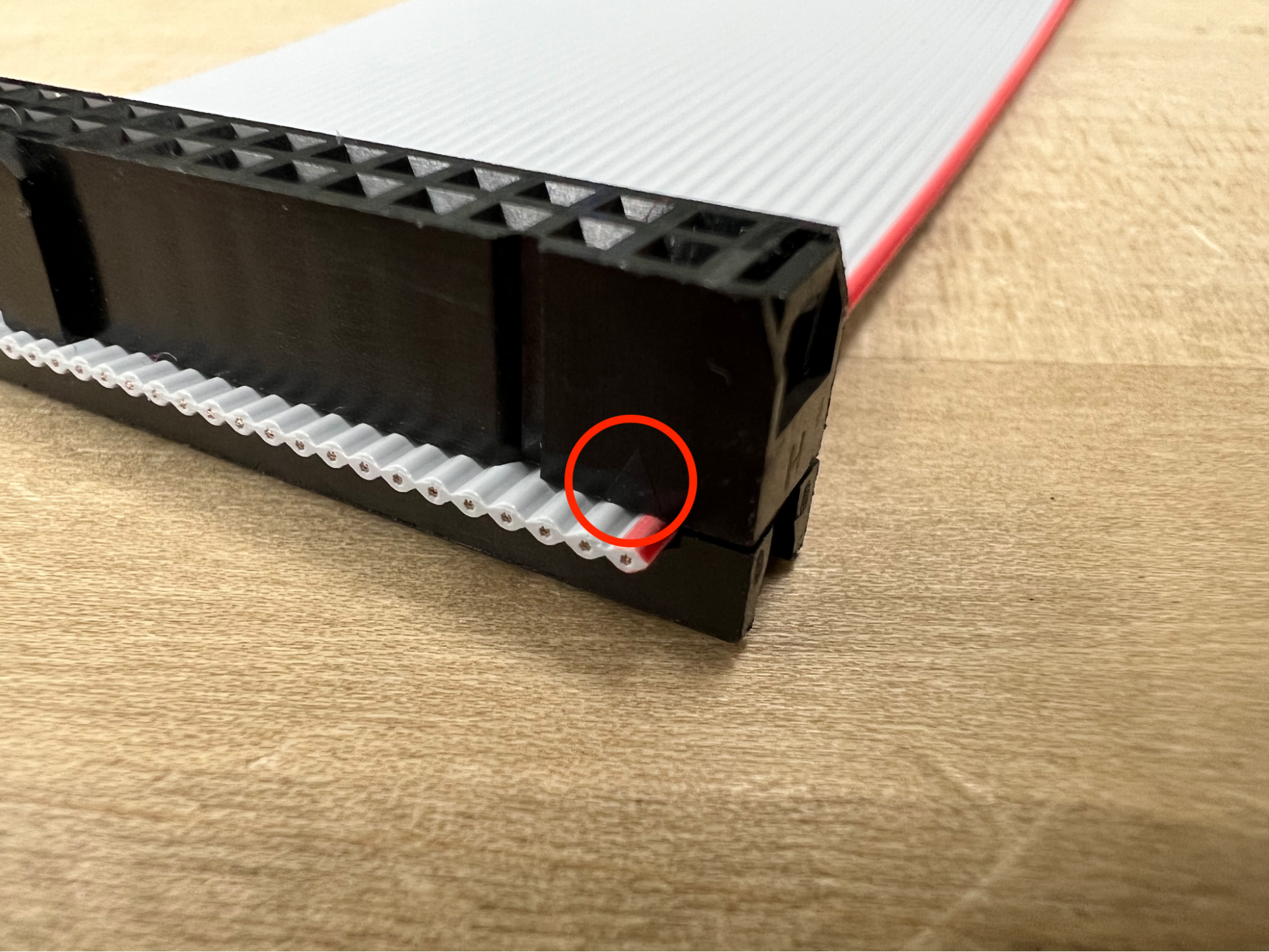
Use the included insulation-displacement contact (IDC) ribbon cable connectors and the spool of ribbon cable in the lab to make yourself a short (~6-12”) cable. You have probably done this before in E80, but if you don’t remember how, see the video here. Cut the cable to length with the flush cutters in the toolbox and use either a vise or the cable assembly tool found in the E155 cabinet. Please make sure to put it back after you are finished. If you can’t find it around the lab, ask an instructor.
Finally, solder the 20-pin male headers and 2x20 pin cable connector onto the breadboard adapter PCB, making sure that the pins are all correctly aligned and perpendicular to the PCB.
Congratulations, you are now finished assembling your board and ready to test it! The photo below shows an example of what the board should look like when it is finished.
Powering the Board
There are three different ways to power the components on the development board: (1) via the VIN power input, (2) via the FPGA’s USB connection, and (3) via the MCU’s USB connection. In this section we will walk through the various ways to power the board to make sure that you are aware of how to properly power the board and avoid any issues which might damage the components on board.
The +5 V and +3.3 V voltage regulators provide power for the various components. All logic levels are +3.3 V unless stated otherwise. So, the +3.3 V supply is used to power the various buttons on the board.
Powering through VIN
To power through VIN, apply a voltage to the power screw terminal between VIN and GND. The NCP117 series can accept voltages up to +20 V but in most scenarios you will likely want to use a VIN between +6-12 V. Be aware that VIN should always be more than +5 V for both regulators to function properly. When powering via VIN, the jumpers J3 (FPGA_+5V) and J4 (MCU_+5V) should be shorted in order to apply the +5 V output from the regulator to the MCU and FPGA +5 V pin.
Powering via USB
It is also possible to power the board via a USB connection to either the MCU or FPGA board. Each board has an onboard voltage regulator to create a stabilized +5 V output on the boards respective +5 V pins. Assuming J3 and J4 are shorted, this +5 V output from whichever board is connected to USB power is fed back to the +5 V line (which is also the output of the +5 V regulator) and thus powers the other components connected to that net.
Testing Voltage Regulators: Before connecting your MCU and FPGA boards, check the voltage regulators are on correctly by connecting to a lab DC power supply using the screw terminals and using a multimeter to confirm that the +3.3 V rail is +3.3 V and the +5 V rail is +5 V. If you read +5 V on the +3.3 V or vice versa, you have installed the regulators in the wrong place and need to swap them. If you read a low voltage (less than ~0.1 V), you likely have a bad solder joint on the back pad of the respective regulator and need to reflow the solder joint to make a better connection.
Testing the Boards
To test the boards, you will upload a simple design to the FPGA which toggles an LED on and off and some code on the MCU to read in the toggling GPIO pin and echo is back to the FPGA. This will ensure that the board is working properly and that you have good communication between the two devices.
To familiarize yourself with how to program the FPGA using Lattice Radiant, see the Lattice Radiant iCE40 UltraPlus Project Setup tutorial. This tutorial has information about how to create a project in Radiant and how to synthesize and upload designs to your FPGA board.
After working through the tutorial, download the Radiant project file fpga_dev_board_test.zip under the Lab 1 subfolder from the course GitHub (the link on the course website lab page) and use it to program your FPGA. This design toggles pin P25 at about 1 Hz. If you have the switch properly set on SW7, P25 is connected to PA9 and so you will see LED D3 blinking.
After programming your FPGA, the next step is to upload the code to the MCU that will read the value of the toggled LED from the FPGA and echo it back on another pin. See the tutorial titled “Segger Embedded Studio Setup” to familiarize yourself with the process of installing and setting up SEGGER Embedded Studio (SES) for ARM. If you are using a lab computer, SES is already installed. Make sure that you use the ARM version of the program. The lab computers may also have other versions installed.
After working through the tutorial, download the SES solution folder from the course GitHub titled “mcu_dev_board_test.zip”. Then, double click on the .emProject file or use the File → Open Solution option in SES to open the solution. This project contains a simple program that monitors the status of PA9 (which is connected to P25 through the appropriate jumper on J5. Make sure you have the jumper attached to connect PA9 to P25). Build and download the project to your MCU.
Now, in addition to LED D3 (PA9/P25) blinking, you should see LED D2 (PA10/P23) and LED D7 (P38) blinking as well.
FPGA Design
Now it’s your turn to take the wheel and create your own design and dust off your digital design chops! Your goal is to write some Verilog modules to further test the hardware on your board and operate a 7-segment display. The system should have the following inputs and outputs:
| Signal Name | Signal Type | Description |
|---|---|---|
clk |
input | 48 MHz clock on FPGA |
s[3:0] |
input | the four DIP switches (on the board, SW6) |
led[2:0] |
output | 3 LEDs (you may use the on-board LEDs) |
seg[6:0] |
output | the segments of a common-anode 7-segment display |
The following tables define the relationship of the LEDs to the switches and clock.
S1 |
S0 |
led[0] |
|---|---|---|
| 0 | 0 | OFF |
| 0 | 1 | ON |
| 1 | 0 | ON |
| 1 | 1 | OFF |
S3 |
S2 |
led[1] |
|---|---|---|
| 0 | 0 | OFF |
| 0 | 1 | OFF |
| 1 | 0 | OFF |
| 1 | 1 | ON |
led[2] |
|---|
| Blink at 2.4 Hz |
Clock Generation To generate the clock for your design, use the onboard high-speed oscillator. This is the same strategy as in the FPGA testing source code you downloaded earlier to test the board. If you look at that Verilog code, you’ll notice an instantiated module called HSOSC (for High-Speed OSCillator). This module is part of the iCE40 Technology Library (see the iCE40 Technology Library document linked on the course website) and is a built-in module included with Lattice Radiant designed for controlling the internal oscillator on the iCE40 chip. You can simply copy the line from the testing program and use it in your project.
Design and Synthesis in Radiant
The 7-segment display should display a single hexadecimal digit specified by s[3:0]. Be sure each digit can be distinguished from other digits (e.g., b and 8 should look different). Remember that you will be using a common anode display. The anode (positive terminal) of all of the LEDs is tied to 3.3 V through a single (“common”) pin. Each segment’s cathode (negative terminal) is connected to a pin. Therefore, you will need 7 separate control signals. Remember that a logic 0 applied to the cathode will turn on the segment. The segments are defined as shown below. Let seg[0] be A and seg[6] be G.

Launch Lattice Radiant and start the New Project Wizard from the File or startup menu. Setup a new project for the UP5K chip following the instructions in the Lattice Radiant Tutorial on the E155 website.
Choose File → New and create a SystemVerilog HDL file. Save the file as lab1_xx.sv in your project directory and check the box to add the file to the current project. Create modules to perform the functions described above. The 7-segment display decoder should be combinational logic. Use a reasonable amount of hierarchy. Name the top-level module lab1_xx. The 7-segment display code, for example, will be reused in future labs, so it should be a module of its own (for the sake of reusability you may want to put this in a separate SystemVerilog file but this is not required). Every module should begin with a comment section that includes your name and email address, the date of creation, and a brief summary of its purpose, so that somebody else can understand what the module does and get a hold of you if they need help with it. Comment the modules as appropriate.
Logic Simulation in ModelSim
The next step is to simulate your logic with ModelSim. Open ModelSim from Radiant from the Tools menu or the icon in the toolbar. The ModelSim window will open. Get in the habit of watching the transcript window to look for errors and to familiarize yourself with what a good run looks like. If you see errors, close ModelSim, correct your Verilog code in Radiant, and reopen ModelSim. You can also edit the file directly in ModelSim and recompile there without going through the entire synthesis pipeline in Radiant.
Note: Some of your designs may include modules from the iCE40 Technology Library (e.g., the HSOSC module we are using to generate our clock signal). If you try to simulate a design including one of these modules, you need to be sure to include the library. When you simulate a design that includes a module from the iCE40 Technology Library, make sure that you include the library by adding under the Libraries tab of the Start Simulation window as shown below.
Starting Simulation
In ModelSim, simulate your module by choosing Simulate → Start Simulation.... Click on the + symbol next to the work library and select your code (lab1_xx).
If the wave pane isn’t open, open it by choosing View → Wave. View all of the inputs and outputs of your design by selecting them in the Objects window and dragging them to the Waves window. In a more complicated design, you may wish to examine internal signals as well.
Manually test your design by forcing the inputs to specific values and then advancing the simulation using “run.” In the transcript window, type:
force s 0000
run 100
force s 0001
run 100
force s 0010
run 100
...
You should see the led and seg outputs displaying appropriate values. Check the outputs against your expectations. If you find any discrepancies, fix the code and resimulate. A helpful shortcut to avoid restarting ModelSim is that you can edit the module by finding it under “work” in the library pane, right clicking, and choosing Edit. Make your fixes, then right click again and choose “Recompile.” Then type “restart -f” in the transcript window to restart simulation without having to set up the waveforms window again. When you return to Radiant, you’ll find your corrected code.
Pin Assignment
Next, assign pins to relate the signal names in your Verilog code to physical pin numbers on the FPGA. Launch Tools → Device Constraint Editor. A table listing all inputs and outputs for the project should appear. Under Pin, type the pin number to associate with the given signal.
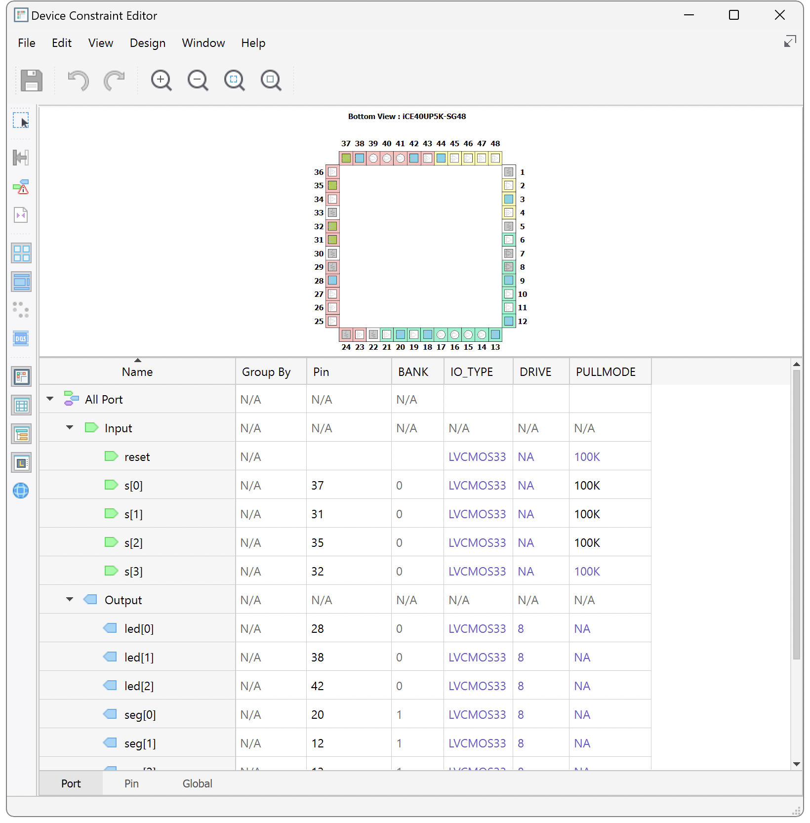
The FPGA pinouts are shown in the Board Schematic. Most of the user input/output (I/O) pins are tapped out to the headers and labeled on the board silk screen. Some have special functions; for example, FPGA pin P42 is connected to LED D6.
The pin numbers for the LEDs and switches are marked on the board’s silkscreen. For the outputs for the 7-segment display, you may select any I/O pins you’d like. Do make sure that these pins are not being used for other purposes.
The Device Constraint Editor is also the place where you can configure the pullup resistors for the I/O pins. To do this, examine the PULLMODE column for any input pins. In your design, this will be the pins connected to s[3:0]. These should be configured with pull-up resistors to avoid invalid logic levels (the exact value is not very important. A value between 10k and 100k is generally sufficient).
Seven Segment Display Circuit
The 7-segment display will be used throughout the class for general output of numbers. In this lab assignment, though, it will be used to output the hexadecimal number entered by the user through the DIP switches.
Each segment of the display works as an independent LED. Therefore, the same current-limiting concern with the LEDs applies to the display as to the on-board bank of LEDs. You can limit the current into each segment of the display the same way you did for the LEDs on board, adding a suitable resistor to provide roughly 5-20 mA of current. You can find resistors and other such components in the supply cabinet or in the stockroom.
Consult the data sheet for the pinout of the common anode dual seven segment display. All seven segments share the same anode, which should be connected to VCC (3.3 V). Each of the segments has its own cathode, which can be pulled to 0 to turn on the segments.
Be sure to turn power off before wiring circuits on your board. You can choose either side of the display to use in this lab. After deciding on which side to use, you will need to connect the VDD pin of that side (either VDD1 or VDD2) to 3.3 V. Then connect the input pins of the same side of the display to the header pins you chose. Remember to add suitable resistors between each of the inputs to the display and the header pins. These LEDs are common anode LEDs. That is, all the anodes from the LEDs are connected to a single VDD (VDD1 or VDD2). You are driving the cathode of each LED. Given this information, you might need to modify your Verilog file. Do so in the simplest way possible.
Generating the FPGA Configuration Files
Now you will synthesize your HDL into a programming file to be transferred onto the FPGA. This outputs a binary file (.bin) in your project directory that can be used to program the FPGA directly over JTAG using the onboard USB programmer. Be sure your SystemVerilog files are saved, and click the green “Play” triangle to start the synthesis process. To help sort the many messages that the compilation process generates, click a tab under the Message area to see only that type of message. If compilation is successful but generates warnings, check the Warning and Error tabs for errors relevant to your design. Warnings about incomplete I/O assignments may be ignored if you have in fact assigned all relevant I/O pins.
Launch Tools → Netlist Analyzer and examine the RTL schematic of your design. This shows the logic synthesized from your Verilog design. Ensure the hardware matches your expectations.
Look at the Reports tab. In the Project Summary under Resource Usage you should see a total number of registers and pins that match your expectations. Under Analysis & Synthesis, you can see how the logic blocks and registers are broken down in each module. Under Fitter, the Pin-Out File should match the pin assignments you intended.
What to Turn In
For this lab and all subsequent ones you will turn in a lab report. The report should not exceed one page of text, plus schematics, code, and anything else appropriate, such as diagrams, simulation results, or calculations. The report typically has the following sections:
- Introduction: Briefly explain what was done.
- Design and Testing Methodology: Explain how you approached the design of this assignment from both a software and a hardware standpoint (as appropriate). Include how you tested your design. These tests should convince the reader that the requirements of the assignment have been met.
- Technical Documentation: Include your Verilog code and schematics of your circuits.
- Quality and clarity of your code is important. Make sure it is adequately commented. Succinct code using standard idioms is best.
- Schematics of your breadboarded circuits should be sufficient for another engineer to understand and reconstruct the circuit on the breadboard. Always use standard symbols for standard components such as resistors, switches, transistors, diodes, etc. Give the component name or part number such that the reader could order parts and replicate your circuit, or look up components in a datasheet where necessary. The reader shouldn’t have to open you HDL synthesis program to relate your Verilog code to the schematic, and shouldn’t need to refer to a data sheet to wire external components or understand what the connections are. Don’t assume that the reader has memorized the pinouts of any chips. Therefore, you’ll need to label both the pin number and pin name for each pin you use from the FPGA board or other component (e.g., 7-segment display). There is no need to draw any of the circuitry on the board; just refer to it by the pins number and name.
- Results and Discussion: Did you accomplish all of the prescribed tasks? If not, what are the shortcomings? How might you address them given more time? As appropriate, how did the design perform (ex. How fast/accurate/reliable was it?). Is there anything you would do differently if you were to redo the lab? Is there anything else interesting worth mentioning?
- Conclusions: Briefly summarize what was done and how it performed.
- How many hours did you spend working on the lab? Any comments, suggestions, or complaints about the assignment? This will not count toward your grade, but will help refine the lab for the future.
The report does not need to be long but should be complete. Some individual questions may not apply to this particular lab but are listed to give you a general idea of what is desired. Future reports will follow a similar format and the questions may be more applicable in these instances.
Have your lab checked off by the instructor. You will need to demonstrate that the board and 7-segment display operate correctly. You will also be asked a question about some part of the lab or your board. You should be thoroughly familiar with all of the lab and the components of your board to be able to answer the question. The oral exam is typically in the form of a “Fault-Tolerance Question.” What would happen if a particular wire is broken or a pin is shorted to Vcc or GND? Be prepared for any other questions about your lab, however.
FAQ and Hints
If some of you are seeing issues with specific pins on your FPGA there could be a few different reasons and corre- sponding steps to take to troubleshoot.
- You could have an electrical short which is causing some pins to be electrically connected that should not due to solder bridges. Double check to make sure that the pins are isolated and not connected together by checking the resistance between the pins with a multimeter.
- You are trying to use a pin that is shared between the FPGA and the MCU and the MCU is not leaving that pin floating or it is driving it as an output. You can get around this by wiping the code on the MCU by uploading a file with a blank main function.
- You should also read through the Nucleo board documentation to see what pins have special functions that are used by default by the MCU. Hint: You likely want to stay away from using the pins that the MCU uses for serial communication by default.
Always Very Curious…
If you finish the lab and are interested in exploring some additional functionality of your FPGA, consider trying to write HDL to control the RGB LEDs on board the UPduino. Note that this is NOT a required part of the lab and not for credit. It is purely an exercise if you have interest!
The UP5K has built in hardware for pulse-width modulation of the LED. To find details on how to use this IP, use the “Lattice Radiant Software Help” guide that is accessible from the Help menu in Radiant. In the window that opens, navigate to the section “Reference Guides > FPGA Libraries Reference Guide > Miscellaneous.” You can also find information about this and other hardware primitives available on the FPGA in the “iCE40 Technology Library” PDF available on the course website. However, note that (annoyingly!) the naming for the modules in this document is for the iCEcube2 software and the syntax has changed for Radiant. You can see the note “Migrating iCEcube2 iCE40 UltraPlus Designs to Lattice Radiant 2.0 Software” for more details.
Footnotes
In order for the NUCLEO board to be compatible with SEGGER, it is necessary to reflash the ST-LINK programmer with SEGGER J-Link firmware to convert it to a J-Link. This has been already taken care of on the board in your kit, but if you want to use another STM32 board with SEGGER you’ll need to follow the instructions here to do this yourself.↩︎