Next: AC equivalent circuits Up: ch4 Previous: Biasing
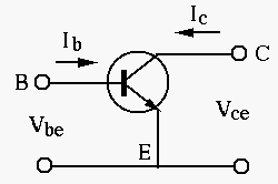
A CE transistor circuit can be modeled by a two-port network as shown below:
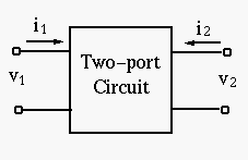
The two-port network is described by the relationship between
two pairs of variables (
 )
associated with the input and output ports. Any two of the four
variables can be assumed to be the independent variables, while
the other treated as the dependent variables, the functions of
the independent variables. In general there are
)
associated with the input and output ports. Any two of the four
variables can be assumed to be the independent variables, while
the other treated as the dependent variables, the functions of
the independent variables. In general there are
![$C_4^2=4!/[2!(4-2)!]=6$](img331.svg) ways to choose any two out of the four
variables. For example, three of these six choices are:
ways to choose any two out of the four
variables. For example, three of these six choices are:
 |
(63) |
 ,
,  ,
,
 , and
, and
 :
:
 |
(64) |
 |
(65) |
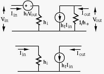
 are the hybrid model parameters:
 : input AC impedance
with
: input AC impedance
with  (output AC short-circuit). This is the AC
resistance between base and emitter, the reciprocal of the
slope of the current-voltage curve of the input characteristics.
(output AC short-circuit). This is the AC
resistance between base and emitter, the reciprocal of the
slope of the current-voltage curve of the input characteristics.
 : reverse transfer voltage
ratio representing how
: reverse transfer voltage
ratio representing how  affects
  with
with  (input
AC open-circuit). In general
(input
AC open-circuit). In general  is small and can be ignored.
 : forward transfer current
ratio or current amplification factor with (output AC
short-circuit). Typically,
: forward transfer current
ratio or current amplification factor with (output AC
short-circuit). Typically,  is in the range of 100 to
200.
is in the range of 100 to
200.
 : output admittance,
with (input AC open-circuit). This is the slope of the
current-voltage curve in the output characteristics. In general
: output admittance,
with (input AC open-circuit). This is the slope of the
current-voltage curve in the output characteristics. In general
 is small and can be ignored.
 , ,
, ,  and are small (
 )
around the DC operating point
)
around the DC operating point  and far away from either the cutoff
or the saturation region, the non-linear quantities that describe the
input and output characteristics can be linearized as the following
small signal model:
and far away from either the cutoff
or the saturation region, the non-linear quantities that describe the
input and output characteristics can be linearized as the following
small signal model:
 |
(66) |
In general,  and are small and could be assumed zero to
further simplify the model (right of the figure above) containing
only two components, a resistor
and are small and could be assumed zero to
further simplify the model (right of the figure above) containing
only two components, a resistor
 and a current source
 .
.
The base and emitter forms a PN-junction with a resistance 
 |
(67) |
 through the PN-junction
between base and emitter. Typically, at room temperature
through the PN-junction
between base and emitter. Typically, at room temperature
 ,
if is approximately in the range of
,
if is approximately in the range of
 , then
is a few hundred ohms.
, then
is a few hundred ohms.
Based on this small signal model, a transistor can be analyzed as a
two-port circuit containing a resistor and a current source
 .
.
In summary, we see that there are two aspects of a transistor circuit:
,  and
and  and voltages
  and
and  ;
;