Next: Small-Signal Model and H Up: ch4 Previous: AC Signal Amplification
As shown before, the DC operating point of a transistor amplification circuit
needs to be set up properly (in the middle of the linear region) to avoid
signal distortion. We now consider how the operating point is determined by
the biasing circuit, in terms of  ,
,  , and
, and  .
.
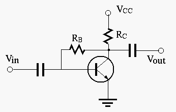
Fixed Biasing
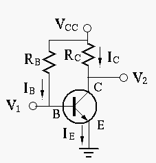
By properly setting the voltage (not too low) and (not too
large), the voltage  can be approximated as a constant value of
 , as shown in the input characteristic plot:
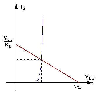
The DC operating point in terms of  and
and  can be
found in the following steps:
can be
found in the following steps:
 |
(29) |
If the transistor is in linear region, then
 |
(30) |
 |
(31) |
and depend on  , which may differ for
different transistors and change depending on the temperatures
the operating point may be unstable and inconsistent.
, which may differ for
different transistors and change depending on the temperatures
the operating point may be unstable and inconsistent.
Example 1
In the fixed biasing transistor circuit shown above,
 ,
,
 ,
,
 , find so that the DC operating point is
in the middle of the linear region of the output characteristic plot, i.e.,
, find so that the DC operating point is
in the middle of the linear region of the output characteristic plot, i.e.,
 . We assume
 (may not be valid if
is too large) and get
(may not be valid if
is too large) and get
 |
(32) |
 to be in the middle of the
load line, we need to have
to be in the middle of the
load line, we need to have
 i.e. i.e. |
(33) |
 to be twice of
at the DC operating point:
to be twice of
at the DC operating point:
 i.e. i.e. |
(34) |
 |
(35) |
Example 2:
In the same circuit above,
 ,
,
,
,
 . Find the operating point
 for
for
 .
.
The load line
 is determined by these two points:


 |
(36) |
values:
 |
(37) |
To minimize distortion, the DC operating point needs to be in the
middle of the load line at
 . But
in this case, we see that
. But
in this case, we see that
 , too close to cutoff region.
, in the middle of linear region as desired.
, too close to cutoff region.
, in the middle of linear region as desired.
 , too close to the saturation region.
The DC operating point of this fixed biasing circuit is not
completely determined by the parameters of the circuit such as
the resistors, as it is also directly affected by factors such
as value and temperature. This situation can be improved
by introducing negative feedback into the circuit.
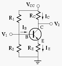
Self-Biasing
To correct the problem above, the self-biasing circuit shown below
can be used to decrease the effect of changing by negative
feed back due to the introduction of  .
.
Qualitatively, an increased (caused by reasons such as
increased due to temperature change) will cause the following
to happen:
 |
(38) |
Quantitatively, we can further carry out analysis of the circuit:
 and
and  are small so that the
current
are small so that the
current  through is much larger than the base current
 i.e.,
i.e.,
 , then the basis voltage
  can be
approximated to be (voltage divider):
can be
approximated to be (voltage divider):
 |
(39) |
 |
(40) |
, we get
 |
(41) |
is independent of , as it is completely
determined by , , and , as well as .
 is not satisfied, the method
above is no longer valid. In this case, we can use Thevenin's theorem
to replace the base circuit by an open circuit voltage
is not satisfied, the method
above is no longer valid. In this case, we can use Thevenin's theorem
to replace the base circuit by an open circuit voltage  (already found above), in series with the internal resistance
  :
:
 |
(42) |
Applying KVL to the base loop we get
 |
(43) |
, we get:
 and and |
(44) |
is not too small (strong negative feedback effect) and
 is not too large (approximately a voltage divider),
so that
is not too large (approximately a voltage divider),
so that
 (e.g.,
 even for a small ), then can be approximated as
 |
(45) |
, and thereby and the DC operating point,
is determined only by the resistors of the circuit, independent of the
. Comparing this with fixed biasing with
 directly proportional to ,
the self-biasing circuit has a much more stable operating point.
directly proportional to ,
the self-biasing circuit has a much more stable operating point.
For this approximation above to be valid, we desire to have smaller
so that is less affected by , and large
for stronger negative feedback. However, as the voltage gain of
the circuit will be reduced due to the negative feedback, cannot
be too large.
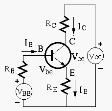
Example 3:
In the circuit of self-biasing,
,
 ,
,
 ,
,
 ,
,
 , Assume
 . The load line is determined by this equation:
 |
(46) |
 and
and
 (short-circuit current)
 and
and
 (open-circuit voltage)
To minimize distortion, the desired operating point should be in the
middle of the load line at
 and
and
 .
.
:
 |
 |
 |
|
 |
 |
 |
|
 |
|
 |
|
 |
|
 |
|
 |
|
 |
|
 |
|
 |
(47) |
 |
|
 |
|
|
|
 |
|
|
|
 |
|
|
|
 |
|
|
|
 |
|
|
|
 |
(48) |
values
can be found to be:
 |
(49) |
We see that in all three cases,
 ,
,
 , i.e., the DC operating point is always
close to the middle of the load line.
, i.e., the DC operating point is always
close to the middle of the load line.
Example 4
In a self-biasing transistor circuit,
 ,
,
 ,
,
, find so that the DC operating point is
in the middle of the linear region of the output characteristic plot.
,
,
, find so that the DC operating point is
in the middle of the linear region of the output characteristic plot.
We first convert the base circuit into its Thevenin's equivalent voltage source composed of
 |
(50) |
 |
(51) |
 |
(52) |
 , and solving the equation we
get
, and solving the equation we
get
 .
.
Example 5
The circuit below shows yet another way to introduce feedback to stablize the DC operating point.
connecting the collector to the base forms
a feedback from the output  to as well as providing
the forward baising needed for the base-emitter PN junction:
to as well as providing
the forward baising needed for the base-emitter PN junction:
 |
(53) |
 |
(54) |
we get
 |
(55) |
 |
(56) |
 (strong negative feedback),
then
(strong negative feedback),
then
 , independent of .
Although typically is significantly greater than ,
the negative feedback still has the tendency to reduce the affect
of varying and thereby stablize the DC operating opint.
, independent of .
Although typically is significantly greater than ,
the negative feedback still has the tendency to reduce the affect
of varying and thereby stablize the DC operating opint.
 , , and a desired
  , find
and so that the DC operating point is in the middle of
the linear region.
, find
and so that the DC operating point is in the middle of
the linear region.
For the DC operating point with to be in the middle
of the linear region, we need
 , and to
be half of the short-circuit current
, and to
be half of the short-circuit current
 ,
we need
,
we need
 |
|
 |
|
|
|
 |
(57) |
 |
(58) |
 |
(59) |
values, which
are all approximately in the middle of the linear region:
 |
(60) |
As discussed above, to avoid distortion of the AC signal,
we desire that the DC operating point is in the middle of
the linear region of the output characterisc, i.e.,
 and
and
 . In
this case, the power consumption is
. In
this case, the power consumption is
 ,
which is the maximum among all possible DC operating points
on the load line:
,
which is the maximum among all possible DC operating points
on the load line:
 |
|
 |
|
 |
|
 |
(61) |
 , and
, and
 |
(62) |