Next: Biasing Up: ch4 Previous: DC Operating Point
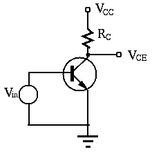
The common-emitter transistor circuit is commonly used for voltage
amplification, as shown in the example below. Here we assume
 and
and
 , and
, and  .
.
The current and voltage on both input and output sides can be obtained either algebraically or graphically as shown below.
The input voltage and current
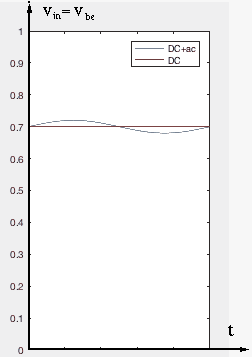
Assuming the transistor is properly biased so that
 ,
we get the input voltage
,
we get the input voltage
 as the superposition
of DC component
as the superposition
of DC component  and a small AC input
 :
:
 |
(22) |
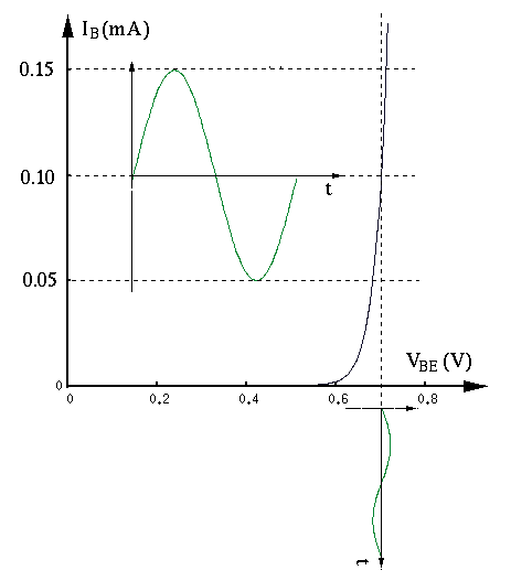
Due to the small dynamic range ( ) of the input voltage, the
non-linear (approximately exponential) input characteristic can be
linearized locally as a resistance, the reciprocal of the
slope of the input characteristic curve around
) of the input voltage, the
non-linear (approximately exponential) input characteristic can be
linearized locally as a resistance, the reciprocal of the
slope of the input characteristic curve around
 :
:
 |
(23) |
 can be approximated to be
 |
(24) |
 and
an AC component with an amplitude
and
an AC component with an amplitude  .
.
Why can't we get the base current in the following way?
 |
(25) |
The output voltage and current
The load line is the plot of equation
 , a
straight line that goes through the two points:
, a
straight line that goes through the two points:
 and and |
(26) |
:
 |
(27) |
 |
(28) |
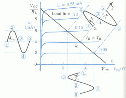
Comparing the AC sinusoidal component
 of
the input and the AC component
of
the input and the AC component
 of the output,
we see that the CE transistor ircuit is a voltage amplifier by which
the input is amplified by
of the output,
we see that the CE transistor ircuit is a voltage amplifier by which
the input is amplified by
 times. Also, the negative
sign indicates the output voltage (
times. Also, the negative
sign indicates the output voltage (
 ) is
) is  out of phase compared to that of the input signal (
 ),
i.e., the circuit is a reverse amplifier.
),
i.e., the circuit is a reverse amplifier.
Waveform distortion
The waveform of the output  may be distorted if the DC component
of the input voltage (and thereby, the base current
may be distorted if the DC component
of the input voltage (and thereby, the base current  ) is
either too low or too high, causing either the positive or negative
peaks of the sinusoidal component to exceed the linear range of the
output characteristic plot, as illustrated below:
) is
either too low or too high, causing either the positive or negative
peaks of the sinusoidal component to exceed the linear range of the
output characteristic plot, as illustrated below:
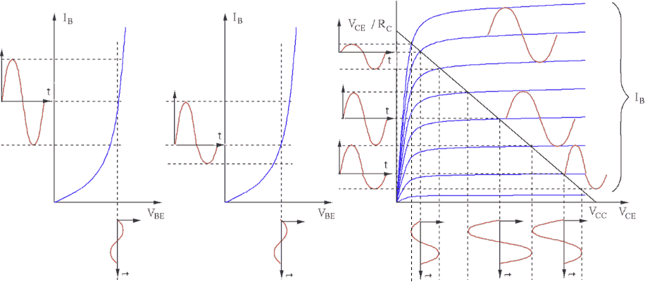
We see that severe distortion in output  will be caused if
a transistor circuit is working near either the cutoff or the
saturation region. It is therefore desirable to properly set the
DC operating point around the middle of the linear range along the
load line, to avoid to be too close to either the saturation or
cutoff region. Specifically,
will be caused if
a transistor circuit is working near either the cutoff or the
saturation region. It is therefore desirable to properly set the
DC operating point around the middle of the linear range along the
load line, to avoid to be too close to either the saturation or
cutoff region. Specifically,
needs to be large enough to avoid distortion due to the
nonlinearity of the input characteristics (close to the cutoff region);
and thereby
 need to be small enough to avoid
distortion due to the nonlinearity of the output characteristics (close
to the saturation region).
need to be small enough to avoid
distortion due to the nonlinearity of the output characteristics (close
to the saturation region).
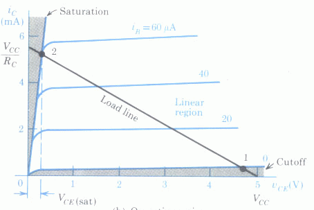
Example
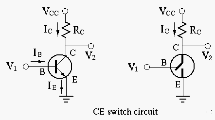
Assume
,
 ,
,  . Given the input voltage
 or
or  , find the corresponding output voltage
 .
.
 , the forward bias of BE PN-junction is insufficient
for it to conduct current, we have
, the forward bias of BE PN-junction is insufficient
for it to conduct current, we have  ,
,
 ,
,
 . The transistor is cutoff (the switch is
open or open-circuit).
. The transistor is cutoff (the switch is
open or open-circuit).
 , the BE PN-junction is forward biased, we can find
from the input characteristics, here assumed to be
, the BE PN-junction is forward biased, we can find
from the input characteristics, here assumed to be  , and get
 and
and
 .
The transistor is in linear region.
.
The transistor is in linear region.
 , the BE junction is forward biased, we can find
from the input characteristics, here assumed to be
, the BE junction is forward biased, we can find
from the input characteristics, here assumed to be  . If the linear
relationship
were to hold, we would get
. If the linear
relationship
were to hold, we would get
 and
and
 .
This result is obviously wrong, indicating that the transistor is actually
in the saturation region (the switch is closed or short-circuit),
i.e., the linear relation
does not hold. In fact, it is
impossible for the transistor to draw
.
This result is obviously wrong, indicating that the transistor is actually
in the saturation region (the switch is closed or short-circuit),
i.e., the linear relation
does not hold. In fact, it is
impossible for the transistor to draw
 from the voltage source,
as the maximum current is
from the voltage source,
as the maximum current is
 when
when
 . In this case, the actual
  can be approximated on the output
characteristics to be about
can be approximated on the output
characteristics to be about  , the intersection of load line and the
curve corresponding to
, the intersection of load line and the
curve corresponding to
 ), and
 .
is only valid when the transistor is in the linear region.
.
is only valid when the transistor is in the linear region.