Next: CMOS Digital Logic Circuits Up: ch4 Previous: Metal-Oxide-Semiconductor Field-Effect Transistors
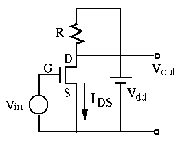
Assume in the circuit above
 and the transistor is in
saturation region, i.e.,
and the transistor is in
saturation region, i.e.,
 , then we have
 |
(160) |
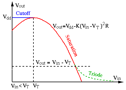
 to the input
  , as
shown by the red segment of the curve in the plot above. As the transistor is
in saturation region,
, as
shown by the red segment of the curve in the plot above. As the transistor is
in saturation region,
 |
(161) |
 to get:
 i.e. i.e. |
(162) |
needs to satisfy both
 and the inequality above, i.e., it
needs to be in the following range:
and the inequality above, i.e., it
needs to be in the following range:
 i.e. i.e. |
(163) |
When the transistor is in saturation mode the slope of the curve (red)
indicates the ratio between input and output , the voltage
gain of the circuit:
 |
(164) |
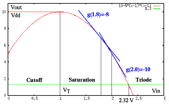
Example: Assume
 ,
,
 ,
,
 ,
,  .
For the transistor to be in saturation region, we need
.
For the transistor to be in saturation region, we need

![$V_{in}<[-1+\sqrt{1+4KRV_{dd}}\;]/2KR+V_T=2.32\;V $](img679.svg)
 |
(165) |
:
 |
(166) |
|
0 | 1 | 1.4 | 1.5 | 1.8 | 1.9 | 2.0 | 2.1 | 2.2 | 2.3 | 2.32 | 2.35 | 2.4 | ||
|
10 | 10 | 9.2 | 8.8 | 6.8 | 6.0 | 5.0 | 4.0 | 2.8 | 1.6 | 1.3 | 0.9 | 0.0 |
increases from  to
to  , the output
decreases from
, the output
decreases from  to
to  , with a gain
 .
Also when the input increases from
.
Also when the input increases from  to
to  , the output
decreases from
, the output
decreases from  to
to  , with a gain
 .
.
In summary, we see that
.
. When
 , the gain
  is greater than one.
 out of phase with the input voltage (
 ),
as the slope of
),
as the slope of
 is negative.
 , the transistor is cutoff. On the other hand, when
 , is more than one
  below , for example,
 ,
,
 , the transistor is in triode
region. In either of the two cases, the transistor has no amplification capability.
, the transistor is in triode
region. In either of the two cases, the transistor has no amplification capability.
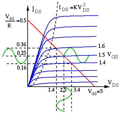
Next we consider a MOSFET circuit with sinusoidal input. Assume the drain resistor
is
 ,
,
 , ,
, ,  and a sinusoidal input
 . If the bias voltage is
 , the
input voltage
, the
input voltage  varies between 1.4V and 1.6V. The output voltage can be
found to be:
varies between 1.4V and 1.6V. The output voltage can be
found to be:
 |
(167) |
 , the output voltage
 and the current
  are, respectively,
 ,
and
,
and
 , as shown in the figure below:
Biasing: In the example above, the DC offset of the input is at 1.5V, so that the transistor is working in the saturation region when the magnitude of the AC input is limited. However, if this offset is either too high or too low, the gate voltage may go beyond the saturation region to enter either the triode or the cutoff region. In either case, the output voltage will be severely distorted, as shown below:
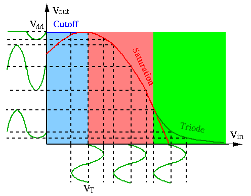
It is therefore clear that the DC offset or biasing gate voltage has to be properly setup to make sure the dynamic range of the input signal is within the saturation region.
Method 1: One way to provide the desired DC offset is to use two resistors
 and
and  that form a voltage divider, as shown in the figure below (a). As
the input resistance of a MOSFET transistor is very high, therefore the gate of
the transistor does not draw any current, the DC offset voltage can simply obtained
as:
that form a voltage divider, as shown in the figure below (a). As
the input resistance of a MOSFET transistor is very high, therefore the gate of
the transistor does not draw any current, the DC offset voltage can simply obtained
as:
 |
(168) |
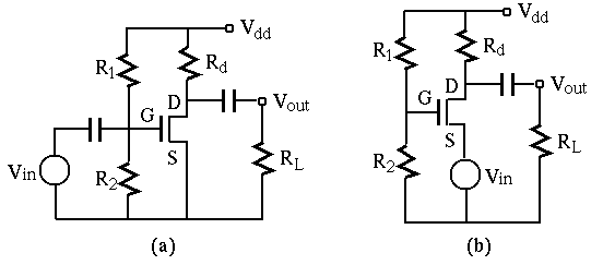
Method 2: Another way to set up the bias is the circuit shown in (b) above.
Assume  ,
,  ,
,  ,
, and
,
, and
 . The bias
voltage can be found to be
. The bias
voltage can be found to be
 , and the voltage between gate and
source is
, and the voltage between gate and
source is
 . The output voltage is
 |
(169) |
 ,
,
 .
.
To determine the dynamic range of the input , recall the conditions for the
transistor to be in saturation region:
 . For this particular circuit,
 |
(170) |
 with corresponding output
 .
.
 . For this particular circuit,
 |
(171) |
 |
(172) |
 |
(173) |
we get
 , with corresponding output

 |
(174) |
 |
(175) |
 . Note that the output voltage is in
phase with the input voltage.
. Note that the output voltage is in
phase with the input voltage.
Source Follower: If the output is taken from the source, instead of the drain of the transistor, the circuit is called a source follower.
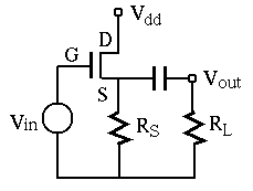
Assume
 , and
, and
 . To find the input and output
voltages and the gain of the circuit, consider the current
. To find the input and output
voltages and the gain of the circuit, consider the current
 :
:
 |
(176) |
 |
(177) |
 , this equation becomes:
 |
(178) |
 or
or
 . We take the smaller
voltage in order for the transistor to be outside the cutoff region:
. We take the smaller
voltage in order for the transistor to be outside the cutoff region:
 |
(179) |
 , the equation becomes:
 |
(180) |
 . The voltage gain of the source follower is
 |
(181) |
To maximize the dynamic range for the input AC signal, the DC operation point
in terms of the DC variables
 needs to be set around
the middle point of the saturation region. If the AC signal around the DC
operation point is small enough, the behavior of the circuit can be linearized
(first term of Taylor expansion of the nonlinear relationship) to simplify the
analysis.
needs to be set around
the middle point of the saturation region. If the AC signal around the DC
operation point is small enough, the behavior of the circuit can be linearized
(first term of Taylor expansion of the nonlinear relationship) to simplify the
analysis.
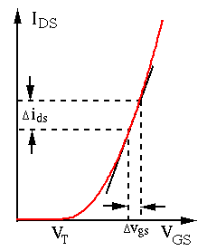
Specifically, the nonlinear relationship between  and
and  can
be linearized around the DC operation point for small changes:
can
be linearized around the DC operation point for small changes:
 |
(182) |
 , called incremental transconductance, is the ratio between small
change in and the small change in .
, called incremental transconductance, is the ratio between small
change in and the small change in .