Next: MOSFET Amplifier Up: ch4 Previous: Colpitts Oscillators
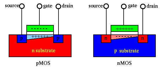
A metal-oxide-semiconductor field-effect transistor (MOSFET) has three terminals,
source, gate, and drain. In an n-MOSFET (or p-MOSFET), both the source S and drain
D are N-type (or P-type) and the substrate between them is P-type (or N-type).
The gate and the P-type substrate is insulated by a thin layer of silicon dioxide
( ). Due to this insulation, there is no gate current to either the source or
drain.
). Due to this insulation, there is no gate current to either the source or
drain.
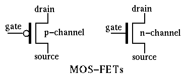
Typically the polarities of the voltages applied to the MOS transistor are such that
 and and |
(154) |
 is applied between gate and source, the
positive potential at the gate will induce enough electrons from the
P-type substrate (minority carriers) to form an electronic channel
called an inversion layer between source and drain, and a current
is applied between gate and source, the
positive potential at the gate will induce enough electrons from the
P-type substrate (minority carriers) to form an electronic channel
called an inversion layer between source and drain, and a current
 between source and drain is formed.
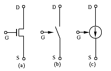
The MOS transistor can be used in either analog circuits or as a switch in binary logic circuit:
 |
(155) |
More acturately, the drain current
 as a function of the
gate voltage can be modeled by
as a function of the
gate voltage can be modeled by
 |
(156) |
is lower than the threshold voltage
 , no inversion layer is formed, and no current flows through S
and D. When is higher than , the current is
proportional to the difference squared.
, no inversion layer is formed, and no current flows through S
and D. When is higher than , the current is
proportional to the difference squared.
Moreover, the current affected by voltage  as well as
can be considered as a function
as well as
can be considered as a function
 of both
and , as plotted below (similar to a bipolar transistor
of both
and , as plotted below (similar to a bipolar transistor
 ):
):
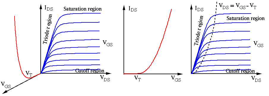
This function can be divided into three different regions:
 and and |
(157) |
 and and |
(158) |
and  at both the S and D ends of the
inversion layer exceeds , some electrons as minority
carriers in the P-type substrate are pulled toward the gate to
form an inversion layer close to the gate to form an N-type
channel with certain resistance between S and D.
increases linearly as increases, with a coefficient
at both the S and D ends of the
inversion layer exceeds , some electrons as minority
carriers in the P-type substrate are pulled toward the gate to
form an inversion layer close to the gate to form an N-type
channel with certain resistance between S and D.
increases linearly as increases, with a coefficient
 (Ohm's law), and nonlinearly as
increases (to pull more electrons toward the gate to enhance the
conductivity of the n-channel). Note that as
(Ohm's law), and nonlinearly as
increases (to pull more electrons toward the gate to enhance the
conductivity of the n-channel). Note that as
 , the
inversion layer is narrower at the D end than the S end.
, the
inversion layer is narrower at the D end than the S end.
but |
(159) |
at the S end exceeds , but at the D
end is lower than . On the one hand, the increased voltage
tends to increase , on the other hand, the reduced
makes the inversion layer at the D end narrow to the extend
that it is nearly closed (pinch-off). As the result, higher
voltage does not cause more current (saturated), and
it is only affected by .
In the plot of vs , the triode region and the saturation
region are separated by the curve of
 .
.
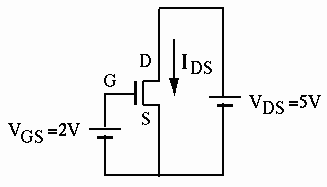
Example: Assume  .
.
 , the MOSFET is in cutoff region with
  independent of .
 and
and
 , the MOSFET is in
linear or triode region with affected by both and .
, the MOSFET is in
linear or triode region with affected by both and .
 , the MOSFET is in saturation region with
determined only by .
, the MOSFET is in saturation region with
determined only by .
Assume
 and , and both MOSFETs in the following
circuit are in the saturation region. Find and output voltage
and , and both MOSFETs in the following
circuit are in the saturation region. Find and output voltage  .
.
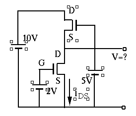
 . As both MOSFETs are in saturation
region with the same which is determined only by but
independent of , their must be the same. The upper
transistor must have the same as the lower one
. As both MOSFETs are in saturation
region with the same which is determined only by but
independent of , their must be the same. The upper
transistor must have the same as the lower one  ,
i.e., the output voltage has to be
,
i.e., the output voltage has to be  . For the lower transistor,
 , i.e., the transistor is indeed in
saturation region.
, i.e., the transistor is indeed in
saturation region.
Comparison between BJT and FET
 . But as MOSFET's gate is
insulated from the channel (
. But as MOSFET's gate is
insulated from the channel (
 ), it draws virtually
no input current from the source and therefore has infinite input
resistance.
), it draws virtually
no input current from the source and therefore has infinite input
resistance.
 is proportional (
 and
and  ) to its input
current (
) to its input
current ( or
or  ), but MOSFET is voltage () controlled.
Consequently, the power consumption of MOSFETs is lower than BJTs.
), but MOSFET is voltage () controlled.
Consequently, the power consumption of MOSFETs is lower than BJTs.
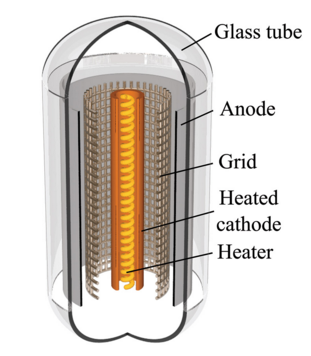
The BJT and FET can be compared with the old technology of vacuum tube based on thermionic electron emission (heated filament). Although the specific physics of each of these devices is quite different from others, the working principles of these devices are essentially the same. In all three devices, a small AC input voltage (signal) is applied to the input terminal of the device (base, gate, or grid) to control the current that flows through the device (from collector, drain, or anode to emitter, source, or cathode, respectively), causing a much amplified voltage to appear at the output terminal (collector, drain, or anode) of the device.