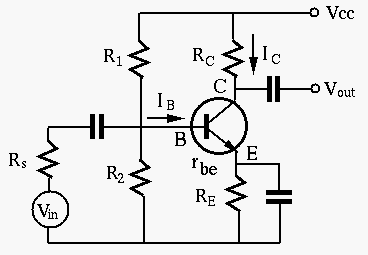
Repeat the above for the amplifier based on a self-biasing
circuit shown in the figure below. Determine the values of  ,
,
 ,
,  , and
, and  to achieve maximum voltage amplification and
minimum distortion by setting the DC operating point to be in the
middle of the linear range of the output characteristic plot.
to achieve maximum voltage amplification and
minimum distortion by setting the DC operating point to be in the
middle of the linear range of the output characteristic plot.
Hint 1: To minimize distortion, the DC operating point
should be around the center of the linear region of the output
characteristic plot, i.e.,
 .
.
Hint 2: write a piece of Matlab code based on the equations for the
self-biasing circuit given
here
to calculates the DC operating point ( ,
,  ,
,  ,
,  ,
,  ,
and
,
and
 ), based on the circuit parameters
  , ,
, and that you choose for your design.
, ,
, and that you choose for your design.
 .
.
- Calculate the DC operating point on the output characteristic
plot (
 and
and  ) based on your design, and compare it
to the actual one measured from the circuit.
) based on your design, and compare it
to the actual one measured from the circuit.
- Test the circuit by a sinusoidal signal of 50 mV peak-to-peak
amplitude from signal generator and an oscilloscope monitor the
input and output signals both before and after the amplification
and to observe the voltage gain and waveform distortion. Compare
the predicted gain based on the small signal model with the actual
one.
- Observe the voltage gain as a function of the by-pass capacitor
in parallel with , and the capacitors at both the input and
output ports, by trying different
 values.
- Observe the voltage gain as a function of the signal frequency.
Generate a Bode plot of the magnitude of the voltage gain for the
frequency range of 10 Hz to 1 MHz. Find the maximum voltage gain
 and the freqnecy range in which this maximum gain is
achieved.
and the freqnecy range in which this maximum gain is
achieved.
- Observe the polarity inversion and the signal distortion.
Increase the amplitude of the input sinusoid from 50 mV to 1 V
and observe the output in terms of the amount of distortion and
clipping at both the positive and negative peaks of the sinusoid.
 .
.