Next: Analysis of Op-Amp Circuits Up: Chapter 5: Operational Amplifiers Previous: Chapter 5: Operational Amplifiers
The circuit schematic of the typical 741 op-amp is shown below:
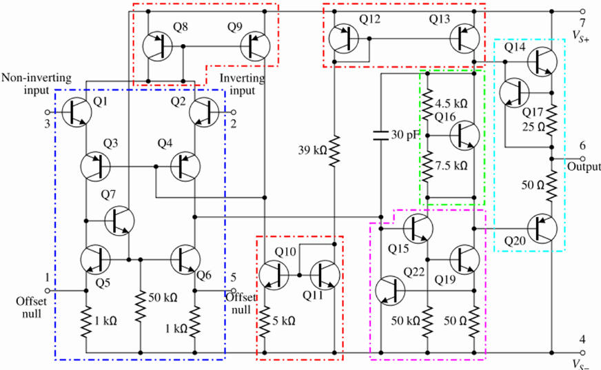
A component-level diagram of the common 741 op-amp. Dotted lines outline:
Like all op-amps, the circuit basically consists of three stages:
 .
.
 of both polarities
(typically
of both polarities
(typically  V).
V).
Although the op-amp circuit may look complicated, the analysis of its operation and behaviors can be simplfied based on the following assumptions:
 can be treated as infinity
 .
.
 ),
and could be approximated to be zero
),
and could be approximated to be zero  .
.
 can be treated as zero
 ,
i.e., the output
,
i.e., the output  is not affected by the load
  (so long as it is
much greater than ).
(so long as it is
much greater than ).
 ), i.e., the property of the op-amp
remain unchanged for all frequencies of interest.
), i.e., the property of the op-amp
remain unchanged for all frequencies of interest.
Based on these approximations, an op-amp can be modeled in terms of the following three parameters:
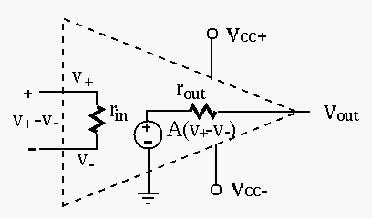
: very large, typically a few mega-Ohms or
higher (
 , e.g., 741
 ), depending on
the frequency and specific components used (e.g., BJT or FET).
), depending on
the frequency and specific components used (e.g., BJT or FET).
:, very small, typically a few tens of
ohms, e.g., 75  .
.
 :, based on both the inverting input
  and the non-inverting input
  :
:
 |
(1) |
 is the differential-mode gain and
  is the common-mode
gain. It is desired that
is the common-mode
gain. It is desired that
 and
and
 ,
i.e., the output is only proportional to the difference between
the two inputs. The common-mode rejection ratio (CMRR) is defined as the
ratio between differential-mode gain and common-mode gain:
,
i.e., the output is only proportional to the difference between
the two inputs. The common-mode rejection ratio (CMRR) is defined as the
ratio between differential-mode gain and common-mode gain:
 |
(2) |
Also, as the output
 is in the range between
  and
and  and
and  is large,
 is small (in the
micro-volt range), i.e.,
is small (in the
micro-volt range), i.e.,
 . If
. If  is grounded as in
some op-amp circuits, then
is grounded as in
some op-amp circuits, then
 is very close to zero, i.e.,
it is almost the same as ground, or
virtual ground.
More generally, even if none of the two inputs is grounded, we can still
assume and are virtually the same to significantly simplify
the analysis of various op-amp circuits.
is very close to zero, i.e.,
it is almost the same as ground, or
virtual ground.
More generally, even if none of the two inputs is grounded, we can still
assume and are virtually the same to significantly simplify
the analysis of various op-amp circuits.
As is large,
 is usually saturated, equal to either
or (called the “rails”), depending on whether or not
is greater than . For
is usually saturated, equal to either
or (called the “rails”), depending on whether or not
is greater than . For  to be meaningful, some kind of
negative feedback is needed. In the following, we consider some typical
op-amp circuits to show how to analyze an Op-amp circuit to find its input
resistance
to be meaningful, some kind of
negative feedback is needed. In the following, we consider some typical
op-amp circuits to show how to analyze an Op-amp circuit to find its input
resistance  , output resistance
  , and open-circuit voltage
gain
, and open-circuit voltage
gain  .
.
, output impedance
and voltage gain , as shown in (B). Then the voltage follower
can be modeled by its input impedance , output impedance ,
and voltage gain , as shown in (C).
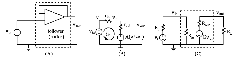
Specifically, , and can be found below. Here
the voltage source in the op-amp is
 .
.
 :
:
Applying KVL to the loop we get
 |
(3) |
 we get the input impedance:
 |
(4) |
:
The open-circuit output voltage is
 |
(5) |
 |
(6) |
 and
and  . We therefore have
 |
(7) |
 :
:
With a short-circuit load  , we have
 , and the
short-circuit current can be found by superposition:
, and the
short-circuit current can be found by superposition:
 |
(8) |
 , we get the output impedance
(Thevenin's model):
, we get the output impedance
(Thevenin's model):
 |
(9) |

In summary, the voltage follower has a unit voltage gain,
but much increased input resistance
 (e.g.,
 ) and much reduced output resistance
 (e.g.,
 ).
In practice we could simply assume
).
In practice we could simply assume
 and
and  .
.
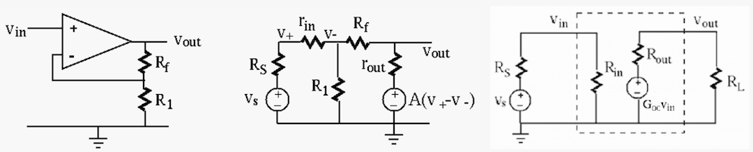
Example:
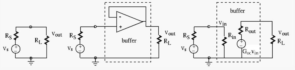
The figure on the left shows a circuit represented by a nonideal
voltage source, containing an ideal voltage source  in series
with an internal resistance
in series
with an internal resistance  (Thevenin's theorem), and a load
. The voltage delivered to the load is (voltage divider):
(Thevenin's theorem), and a load
. The voltage delivered to the load is (voltage divider):
 |
(10) |
due to the voltage drop
 across the internal resistance . For the
doutput voltage to be as close to the source as possible, the internal
resistance needs to be small compared to the load resistance .
across the internal resistance . For the
doutput voltage to be as close to the source as possible, the internal
resistance needs to be small compared to the load resistance .
In the middle figure, a voltage follower (as a buffer) is inserted in
between the source and the load. The follower is modeled by its input
and output resistances and , as well as its voltage
gain , as shown in the right figure. The output voltage can be
obtained after two levels of voltage dividers:
 |
(11) |


 |
(12) |
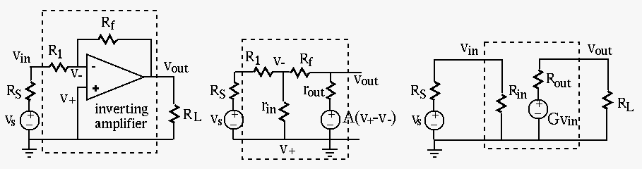
To simplify the analysis of the circuit based on the full model of the op-amp, we make certain approximations in the following.
 )
)
As
 , we approximate
 and
. We have
and
. We have
 and
and
 ,
and get
,
and get
 |
(13) |
we get
 |
(14) |
![$\displaystyle v_{out}=v_{in}-(R_1+R_f) i_{in}
=v_{in}\left[1-\frac{(A+1)(R_1+R_f)}{(A+1)R_1+R_f}\right]
=v_{in}\frac{-AR_f}{(A+1)R_1+R_f}$](img77.svg) |
(15) |
 , we get the open-circuit voltage gain:
 |
(16) |
.
This result can also be obtained under the virtual ground assumption
. Applying KCL at the node of , we get
 i.e. i.e. |
(17) |
We find the input resistance as the ratio of
and the input current . By KCL applied to the node of
:
 |
(18) |
:
 |
(19) |
 |
 |
![$\displaystyle \frac{v_{in}-v^-}{R_1}
=\frac{v_{in}}{R_1}\left[1-\frac{R_f}{R_f+(A+1)R_1}\right]$](img86.svg) |
|
|
 |
(20) |
by we get
Note that this input resistance is significantly smaller
than that of the voltage follower with
!
):
 |
(22) |
 , the above becomes
 |
(23) |
we get
 |
(24) |
we get
 |
(25) |
 |
|
![$\displaystyle [v^--(-Av^-)]\frac{r_{out}}{R_f+r_{out}}-Av^-
=v^-\left[(1+A)\frac{r_{out}}{R_f+r_{out}}-A\right]$](img95.svg) |
|
|
 |
(26) |
 |
|
 |
|
 |
 |
(27) |
and
 .
.
In summary,
 |
(28) |
 |
(29) |
 |
(30) |
The three parameters of this non-inverting amplifier can be found to be (see here):
 |
(31) |
 |
(32) |
 |
(33) |
 , but smaller and bigger
. In particular if
, but smaller and bigger
. In particular if  , this non-inverting amplifier
becomes a voltage follower with
, this non-inverting amplifier
becomes a voltage follower with  ,
,
 , and
, and
 .
.
