Note: in the figure above, as the assumed polarities of both ![]() and
and
![]() are the opposite to those assumed in plot (b) below, the negative
signs for both
are the opposite to those assumed in plot (b) below, the negative
signs for both ![]() and
and ![]() in the plot should be dropped.
in the plot should be dropped.
Solution:
![]() ,
,
![]() ,
,
![]() , or
, or
![]() .
.
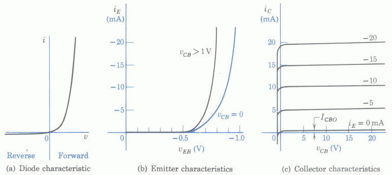
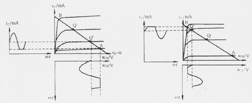
If ![]() and
and ![]() ,
, ![]() can be estimated from
figure (b), and correspondingly,
can be estimated from
figure (b), and correspondingly, ![]() and
and ![]() . When
. When
![]() ,
, ![]() ,
, ![]() , and
, and ![]() .
.
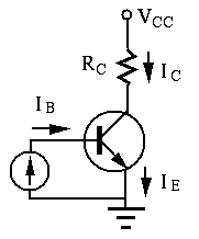
Solution:
Solution: The load line goes through the points
![]() and
and
![]() .
Its intersection with the curve
.
Its intersection with the curve ![]() is approximately at
is approximately at
![]() , where we can also find
, where we can also find
![]() and
and
![]() .
.
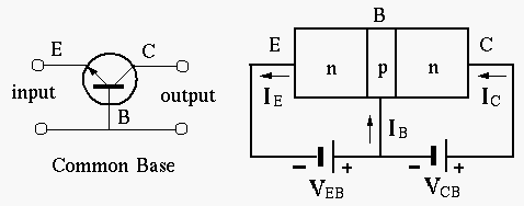
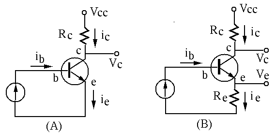
Note: As the convention in the schematics of transistor circuits,
the bottom horizontal line is treated as the ground, and all voltages,
such as ![]() ,
, ![]() and
and ![]() are measured with respect to the
ground as the reference point.
are measured with respect to the
ground as the reference point.
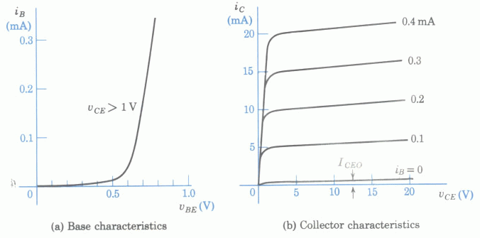
Hint: The relationship ![]() is only valid in the
linear region in the middle range of the load line. However, in
the cut-off region (close to the horizontal axis) and the saturation
region (close to the vertical axis), the above relationship no
longer holds and the actual output current
is only valid in the
linear region in the middle range of the load line. However, in
the cut-off region (close to the horizontal axis) and the saturation
region (close to the vertical axis), the above relationship no
longer holds and the actual output current ![]() and
and ![]() can
only be found graphically in the output characteristic plot.
can
only be found graphically in the output characteristic plot.
Solution:
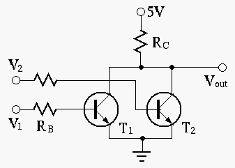
Solution: When ![]() ,
, ![]() is cut-off. When
is cut-off. When ![]() ,
,
![]() ,
, ![]() is saturated with
is saturated with ![]() and
and
![]() (instead of
(instead of
![]() ).
The same is true for
).
The same is true for ![]() . From the table below we see that the
circuit is a NOR (not OR) gate (high voltage for True and low
voltage for False).
. From the table below we see that the
circuit is a NOR (not OR) gate (high voltage for True and low
voltage for False).