JTAG Programmer and Hardware Debugger
Final Project Report
December 7, 1999
E157
Stephani Ordinario and April Fields
Abstract:
Due to the increasing pressure to decrease the size of printed circuit boards, the Joint Test Action Group (JTAG) created a standard for on-chip, built-in test circuitry to allow testing of boards without the necessity of physically probing every miniscule connection. Xilinx has taken this standard one step further and used JTAG to allow users to program and test FPGAs and the boards they are designed for, directly from a PC. This programming process is intended to assist in debugging a prototype design. This project performs and documents the various functions of Xilinx’s JTAG capabilities.
Introduction
The current process for programming FPGAs for microprocessor labs in unnecessarily time consuming due to the poor state of the debugging process. As it stands, the two most successful methods for debugging are the Xilinx simulator which tests your program in software (as opposed to testing the actual function of your program) and the logic probe, which can only check hardware you can physically access and only one pin at a time.
There exist two hardware/software tools that might aid microprocessor lab students by greatly reducing debug time.
The first is the JTAG Programmer software and Xchecker or Parallel cable. Either cable can be used to access just four FPGA pins. The JTAG Programmer can program an FPGA in 2.22 seconds directly from a PC without an EEPROM. Using JTAG Programmer would allow a student to make continuous changes to their Xilinx programs and try them on their board immediately without having to waste time copying files to disk running upstairs, and programming an EEPROM.
The second tool is the Hardware Debugger software and the Xchecker cable which requires nine pins on the FPGA. The Hardware Debugger can program an FPGA, though it takes a bit longer, and it can also display waveforms for any net (or all of them) in an FPGA after programming. This would greatly increase debugging capabilities by allowing students to see what their FPGA is actually doing internally.
All of this functionality can be added to microprocessors lab with a minimal amount of change to an FPGA program and the board hardware.
New Hardware
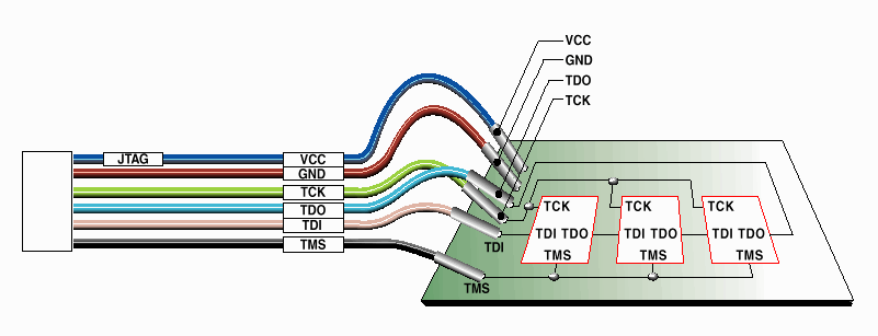 Programming and testing in JTAG Programmer requires the use of either a Parallel Cable or a serial Xchecker cable. Each cable consists of one end that plugs into the serial or parallel port of a PC and another end that holds many flying leads that are attached at various positions to the FPGA. See Figure 1 for a diagram of the parallel cable.
Schematics
In order to try out the capabilities of JTAG, we programmed our E157 boards with just an inverter and a flip-flop.
A few changes to the E157 board were required to enable JTAG Programmer. The resistors that tie TCK and INITB high must be clipped and a 1kW
resistor added to tie INITB low. To program with Hardware Debugger, the resistor tied to the MODE pin of the FPGA, which sets the FPGA to master serial mode, must be clipped, resetting it to slave serial mode. The 1kW
INITB resistor used for JTAG Programmer must be removed.
It is easy to modify the board to allow for EEPROM, JTAG and Hardware Debugger programming. One possible configuration is pictured in the schematic in Appendix A.
FPGA Design
JTAG Programmer
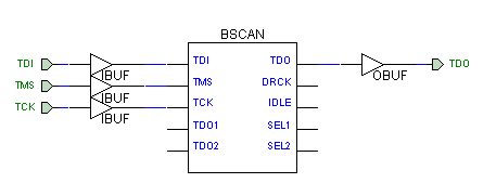 It is possible to program an FPGA, using JTAG Programmer, without making any modifications to the FPGA design. There is flaw, however in JTAG Programmer which causes it to stop programming before the registers are initialized. So, when there are registers in the design, the pre-designed macro BSCAN must be added into the design. This can be done in either schematic or verilog. In figure 2 below, BSCAN has been incorporated into a simple circuit schematic.
The code required to do the same process in Verilog is:
input TDI, TMS, TCK;
output TDO;
wire tck_net, tdi_net, tms_net, tdo_net;
BSCAN u1 (.TDI(tdi_net), .TMS(tms_net), .TCK(tck_net), .TDO(tdo_net));
TDI u2(.I(tdi_net));
TMS u3(.I(tms_net));
TCK u4(.I(tck_net));
TDO u5(.O(tdo_net));
Hardware Debugger
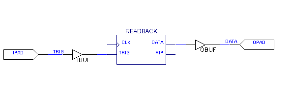 Hardware Debugger can not only program an FPGA, it can read back values for any net in the FPGA. Hardware Debugger requires the BSCAN symbol used for JTAG and a second symbol called READBACK, the schematic of which is shown in Figure 3.
The code required to include Readback capabilities in Verilog is:
input rt, clk;
output rd, rip_p;
RDBK U0 (.TRIG(rt), .DATA(rd), .RIP(rip_p));
RDCLK U1 (.I(clk));
Results
Implementing the necessary additions for JTAG programming is pretty simple and programming time is very short. There are a number of funny quirks and little things to remember. For example, you have to reset the FPGA before you reprogram because the software can’t do it and if you reset the FPGA, you have to reset the cable in the software. It doesn’t take long, however, to become familiar with these issues once the setup is correct.
Hardware debugger is designed to help while working on an FPGA prototype. The possibility of accessing internal nets could be very beneficial. Hardware Debugger is pretty limited in its readback capabilities. It can only take snapshots at a rate of one per second (which doesn’t appear to be adjustable). So any clock signals or other signals that are expected to change during a one-second duration are recorded as being at the same level over the whole second. The level is whatever level the signal was at when the snapshot was taken. Also, Hardware Debugger can only use the Xchecker cable and is much slower and requires access to more of the FPGA pins.
References
- Spartan and SpartanXL Families Field Programmable Gate Arrays, http://www.xilinx.com/partinfo/spartan.pdf
- http://www.xilinx.com/support/techsup/journals/jtag/start.htm
- READBACK Component, Xilinx Development System, http://support.xilinx.com/support/sw_manuals/2_1i/download/docawsg.pdf
- Instantiating Readback in Verilog, http://www.xilinx.com/techdocs/3595.htm
- Instantiating BSCAN in Verilog,
http://www.xilinx.com/techdocs/488.htm
Hardware Debugger Guide, http://toolbox.xilinx.com/docsan/2_1i/data/common/hdb/hdb1_3.htm
Data Generation and Configuration for Spartan Series FPGAs, http://www.xilinx.com/apps/xapp.htm
*This was the good Readback one with the Readback diagram we actually ended up using.
JTAG Programmer Guide, http://www.xilinx.com/support/sw_manuals/2_1i/download/jtag.pdf
Boundary Scan in XC4000, Spartan, and XC52000 Series Devices, http://www.xilinx.com/xapp/xapp017.pdf