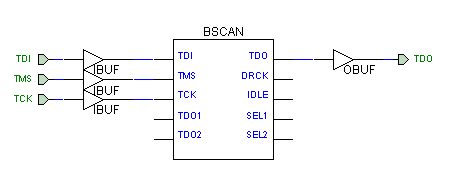
 In Schematic Editor, add the symbol name BSCAN. Attach it according to Figure 1 below. Even if this is going into your top-level schematic, do not put IPADs and OPADs onto BSCAN; just use ports given the same name as the pins in BSCAN.
JTAG Programmer
and
Hardware Debugger
Manual
April Fields
Stephani Ordinario
E157
December 7, 1999
I. Programming with JTAG Programmer
JTAG Programmer allows you to program your FPGA directly from the PC, avoiding programming with EEPROM. This is most helpful during the debugging stages. Rather than converting all the files and running up and down stairs, you can easily alter your FPGA files and program them immediately.
The E157 board is designed for programming FPGAs using EEPROMs. Therefore, it has a resistor tying INITB high. In order to allow programming via JTAG, a 1kW resister must be placed on your protoboard tying INITB to ground.
Both the Xchecker (serial) and Parallel Cables use four Test Access Port (TAP) pins (Table 1.) and Vcc and GND connections (for JTAG, not FPGA on Parallel cable). These connections can be made on the protoboard at their corresponding pins. The other side of the cable plugs into the port on the back of the computer.
|
Name |
Function |
|
TDO (RD) : Test Data Out (Read Data) |
Reads the Readback data |
|
TDI : Test Data In |
Transmits serial data |
|
TCK : Test Clock |
Clocks the test logic for devices on boundary-scan chain |
|
TMS : Test Mode Select |
Controls state of the TAP Controller |
Table 1. TAP pins needed for JTAG
Attach your board to the 5V power supply and turn it on.
It is possible to program your FPGA using JTAG without making any modifications to your design. There is flaw, however, in JTAG Programmer which causes it to stop programming before the registers are initialized. So, if there are registers in your design, you need to add a pre-designed macro to your design. This can be done in either schematic or Verilog.
In Schematic Editor, add the symbol name BSCAN. Attach it according to Figure 1 below. Even if this is going into your top-level schematic, do not put IPADs and OPADs onto BSCAN; just use ports given the same name as the pins in BSCAN.
Figure 1. BSCAN symbol
In HDL Editor, add the following code into your Verilog files:
input TDI, TMS, TCK;
output TDO;
wire tck_net, tdi_net, tms_net, tdo_net;
BSCAN u1 (.TDI(tdi_net), .TMS(tms_net), .TCK(tck_net), .TDO(tdo_net));
TDI u2(.I(tdi_net));
TMS u3(.I(tms_net));
TCK u4(.I(tck_net));
TDO u5(.O(tdo_net));
Remember that Verilog is case sensitive. This code must be added to your top-level module.
C. Using JTAG Programmer
Once the board and program files are ready, you can program your FPGA. Proceed as usual through the Implementation phase in Xilinx Foundation. When
implementation is complete, click on the Program button in the main window. This 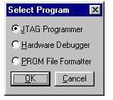 brings up a menu of programming methods.
Figure 2. Select JTAG Programmer
Select JTAG Programmer. The JTAG Programmer software package will open and it should automatically load an FPGA symbol which should be correctly listed as XCS10_PC84 and it should have your file to be programmed listed as a bit file below the FPGA.
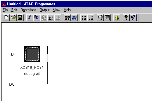 Figure 3. JTAG Programmer
The bit files are Xilinx FPGA Configuration files that Xilinx Foundation generates. If any of these steps does not happen automatically or happens incorrectly, click on the FPGA and follow the steps to load the correct bit file.
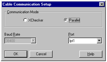
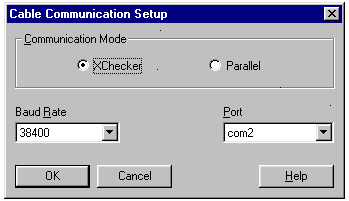
Figure 4. Cable Communication Setup with (a)Xchecker and (b)Parallel Cables
You can select Xchecker or Parallel as the Communication Mode depending on which cable you’ve chosen. Either will work with JTAG Programmer. You also select the Port that you plugged the cable into on the back of your computer. If you are using an Xchecker cable the baud rate is adjustable. Once you’ve selected your cable settings, click OK. Make sure that the power is ON before you do this, otherwise the program will not be able to establish a connection. Also make sure not to turn the power off anytime during programming because this will cause errors. This is because the FPGA reconfigures every time it gets powered up and it loses the program every time it gets turned OFF. If the power is shut down, you must reset the FPGA and the cable.
Click on the FPGA symbol to highlight it. The FPGA symbol needs to be highlighted in order to program it. Click on Operations/Verify and then click OK. If you get errors, it is most likely a connection error with the cable or your FPGA is already programmed (in this case, just hit the reset key) or it may not be able to find the Boundary-Scan Description Language (BSDL) file. The BSDL file describes the boundary scan features of the FPGA and is required for programming. Xilinx Foundation should have the BSDL files already where the file name is just XCS10_PC84.bsd. Sometimes Xilinx Foundation can be flaky and you simply have to find the file and open the folder where it’s located and then retry Verifying.
Now you can program your FPGA! Click on Operations/Program and a program window will pop up.
Click OK. If the prompt says your device has programmed successfully, you’re done. You can even disconnect the Xchecker or parallel cable from your board. Just remember that once you turn the power off, your FPGA won’t remember the program because it reconfigures on power up.
II. Using Hardware Debugger
Hardware debugger also allows you to program your FPGA directly from the PC. Currently, the only cable which allows you to program with Hardware Debugger is the Xchecker cable. This is because the Xchecker cable is the only cable which has readback capabilities.
A. Hardware Setup
As mentioned before, the E157 board is designed for programming FPGAs using EEPROMs. Therefore, there are resistors tying MODE low. In order to program sing Hardware Debugger, this resistor must be clipped from the board.
Using the Xchecker cable, make the appropriate Vcc and GND connections. The other side of the cable plugs into the port on the back of the computer. Also make the following connections to your protoboard*:
|
Xchecker lead |
E157 Board Pin |
|
RD |
DATA (check ucf file, you must declare this pin) |
|
CLKI |
MCLK |
|
CLKO |
clk0 (check ucf file, you must declare this pin) Note: even if this is called clk in your Verilog code, it will be called clk0 in the ucf file. |
|
RT |
TRIG (check ucf file, you must declare this pin) |
|
PROG |
PROGB |
|
INIT |
INITB |
|
DIN |
DIN |
|
CCLK |
CCLK |
|
D/P |
DONE |
Table 2. Connections needed for Hardware Debugger
*Any Xchecker leads not mentioned should not be connected.
Attach your board to the 5V power supply and turn it on.
B. FPGA Design Considerations
In order to program using Hardware Debugger, you do not need to include READBACK. However, if you wish to use the Waveform Generator you must include READBACK. And if there are registers in your design you must also include BSCAN. (See section I.B. for instructions on including BSCAN)
To add READBACK in Schematic Editor, just add the symbol named READBACK. Attach an IPAD and OPAD to the TRIG and DATA pins, respectively. It should look like Figure 6 below. This symbol needs to be added to your top-level schematic.
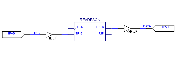 Figure 6. READBACK symbol
In HDL Editor, add the following Verilog code:
input rt, clk;
output rd, rip_p;
RDBK U0 (.TRIG(rt), .DATA(rd), .RIP(rip_p));
RDCLK U1 (.I(clk));
Be aware that Verilog is case sensitive. The preceding code must be included in your top-level module if you wish to use Readback.
C. Using Hardware Debugger
Once the board and program files are ready, you can program your FPGA. Proceed as usual through the Implementation phase in Xilinx Foundation. When implementation is complete, click on the Program button in the main window of Program Manager. This
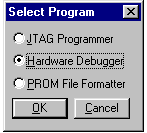
Figure 7. Select Hardware Debugger
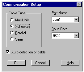
Figure 8. Communication Setup window
Select the Cable Type, Port Name, and Baud Rate and then click OK. The Hardware Debugger software package will then open.
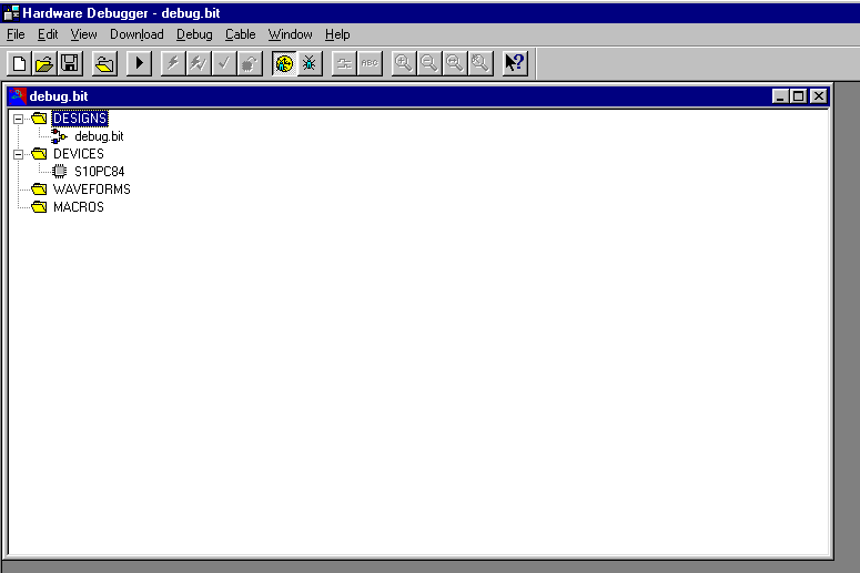 Figure 9. Hardware Debugger
To program your FPGA, go to Download/Download Design. Once it’s done programming your FPGA a message should pop up saying that your device is now configured.
To use Readback, go to Debug/Settings/Trigger and select ‘immediately’ in the drop box. Then go to Debug/Settings/Display Signals.
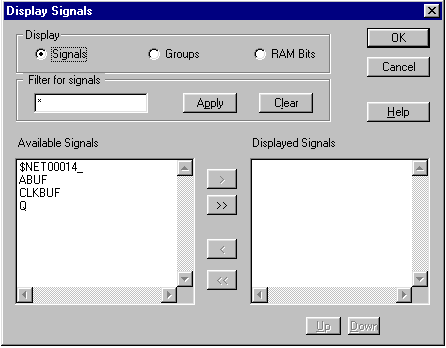
Double click on all of the available signals that you want to be able to readback. Click OK. A Debug Control Panel box will open now. Click on Clock and select CLKI . Click OK and Waveform1 will open.
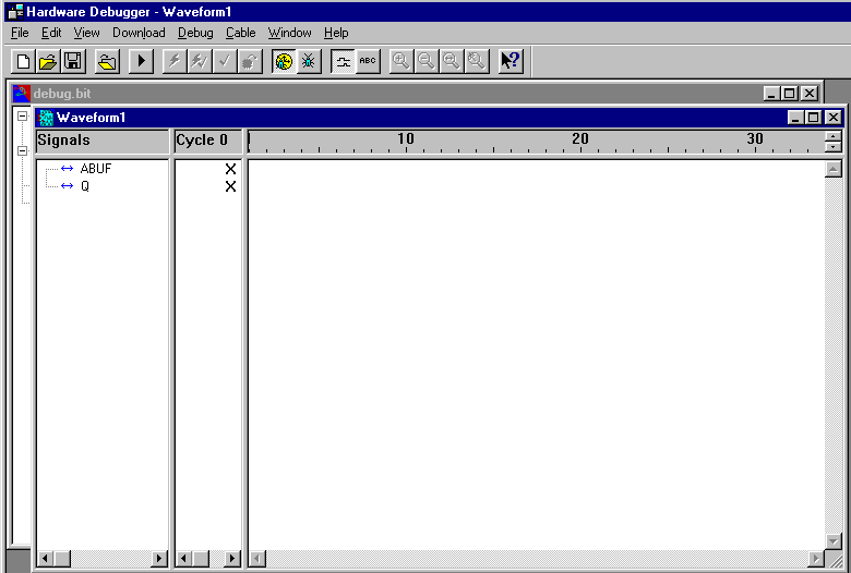 Figure 11. Waveform window
To readback snapshots of the signals you selected, go to Debug/Settings/Read Snapshots.
To change the number of snapshots taken at one time, go to Debug/Settings/Number of Snapshots to Read. To change the color of a particular wave, right click on the signal name and select to change color.
Have fun debugging!